Showing posts with label AI Chip. Show all posts

Intel Launches Starfire: AI‑Powered Chip to Transform Space Computing

Intel Launches Starfire: AI‑Powered Chip to Transform Space Computing

Intel has unveiled Starfire, its first space‑grade chip built on the advanced Intel 18A process, designed to power AI workloads directly aboard satellites and spacecraft. The processor is engineered to withstand radiation, extreme temperatures, and long missions, marking Intel’s bold entry into the aerospace computing market.

Currently, most satellites and spacecraft use  radiation‑hardened processors like BAE Systems’ RAD750 and RAD5545, but newer missions are increasingly adopting commercial off‑the‑shelf (COTS) chips such as NVIDIA Jetson Orin and ARM‑based SoCs for AI workloads. NASA and Microchip are also developing next‑generation high‑performance spaceflight computing systems.

The space computing market has long relied on BAE Systems’ RAD750 and RAD5545, with Microchip developing NASA’s next‑gen processor. Starfire is Intel’s bid to disrupt this dominance.

Starfire chip was developed under Intel Government Technologies with strong alignment to U.S. defense and aerospace programs, but it is not restricted to government use alone. While U.S. manufacturing and security programs are central, Intel has signaled broader availability for international partners once qualification is complete.

Starfire is part of Pentagon‑linked initiatives like RAMP‑C and SHIP, ensuring trusted supply chains and radiation‑hardening standards. Intel has positioned Starfire for private operators who want onboard AI inference for navigation, imaging, and scientific data processing.

Starfire is designed first for U.S. government and defense applications, but Intel intends it to be a dual‑use technology — serving both national security and commercial satellite markets worldwide. Its U.S. manufacturing under the Trusted Foundry program ensures compliance with defense standards, while its AI capabilities make it attractive for global space operators.

Key Highlights of Intel’s Starfire Chip

  • Space‑grade design: Built to survive radiation, thermal cycling, and 10+ year missions in orbit.
  • AI acceleration: Up to 75 TOPS of performance via a three‑tile neural processing unit.
  • CPU architecture: Eight cores (4 performance + 4 efficiency) on Intel’s 18A node.
  • GPU integration: Four‑core Xe GPU with 64 execution units, built on Intel 3.
  • Packaging: Uses Intel’s Foveros 3D stacking for compact, resilient design.
  • Variants: Low‑power (10 W, up to 45 TOPS) and Performance (35 W, up to 75 TOPS).

Key Specs from Intel Starfire Datasheet

FeatureDetails
CPU8 cores (4 performance + 4 efficiency) on Intel 18A
GPU4 Xe cores, 64 execution units (Intel 3)
NPU3‑tile design, up to 75 TOPS
MemoryLPDDR5 / DDR5 support
Connectivity12 PCIe Gen4 lanes
Thermal Range−55°C to 125°C
Mission Life10+ years
Source - Intel 

Comparison: Starfire vs Legacy Space Chips

ChipPerformanceProcess NodeAI CapabilityMission Lifespan
Intel StarfireUp to 75 TOPSIntel 18A (CPU/NPU), Intel 3 (GPU)Dedicated NPU for AI inference10+ years
BAE RAD750110–200 MHz150–250 nmNoneProven on Mars rovers
BAE RAD5545Multi‑core, higher throughputMature nodeLimitedLong‑duration missions
NASA/Microchip Next‑Gen100× current throughput (in development)TBDAI‑readyFuture missions

Strategic Impact

  • National Security: Aligns with U.S. government’s emphasis on space as a defense domain.
  • Commercial Satellites: Enables autonomous navigation, onboard image processing, and scientific data analysis without ground reliance.
  • Market Disruption: Competes with aerospace chips like BAE’s RAD750, offering modern AI capabilities.

Challenges & Risks

  • Radiation qualification pending: Validation against total ionizing dose and single‑event effects still in progress.
  • Yield concerns: Intel’s 18A node may face production yield issues until 2027.
  • Adoption timeline: Engineering samples ship in Q3 2026, broader deployment post‑qualification.

Bottom Line

Intel’s Starfire chip represents a major leap in space computing, bringing modern AI and high‑performance processing into orbit. If radiation testing succeeds, it could redefine how satellites and spacecraft handle data, shifting from ground‑based reliance to autonomous, onboard intelligence.

Anthropic Eyes Samsung Partnership to Build Next-Gen AI Chips

Anthropic Eyes Samsung Partnership to Build Next-Gen AI Chips

Anthropic has entered preliminary talks with Samsung to manufacture a custom AI chip using Samsung’s advanced 2nm process, a move that could reshape the AI hardware landscape by reducing dependence on Nvidia and optimizing costs for running Claude at scale. While no design or production timeline has been finalized, the discussions highlight Anthropic’s ambition to build in-house silicon expertise and Samsung’s push to challenge TSMC in cutting-edge foundry services. 

Anthropic’s Strategic Shift

Anthropic, valued at nearly $965 billion, is exploring custom silicon as part of a broader industry trend where leading AI labs seek control over their hardware supply chains.
The company has begun defining specifications for a processor that could handle inference workloads—the computationally intensive task of running large language models like Claude—rather than training, which remains dominated by Nvidia GPUs and Google TPUs. This mirrors OpenAI’s unveiling of its Broadcom-designed “Jalapeño” inference accelerator.

The hiring of Clive Chan, a key engineer from OpenAI’s chip team, underscores Anthropic’s intent.

Chan helped design Jalapeño and brings expertise in building accelerators from the software layer up, giving Anthropic a strong foundation for its own silicon program.

Why Samsung?

Samsung’s appeal lies in both financial alignment and manufacturing capability.
The company participated in Anthropic’s $65 billion Series H round in May 2026, alongside SK Hynix and Micron, but unlike those firms, Samsung operates a foundry capable of producing advanced logic chips.

The talks focus on Samsung’s SF2 2nm process, which uses Gate-All-Around (GAA) nanosheet transistors for improved efficiency and density, and its advanced packaging technology, critical for high-bandwidth connections between logic and memory.

If successful, Anthropic would become a marquee client for Samsung Foundry, bolstering its bid to compete with TSMC, the current leader in advanced semiconductor manufacturing.

Industry Context

The move reflects a broader diversification trend in AI hardware.

Nvidia currently controls about 74% of the AI chip market, but soaring GPU costs—H100 units sell for over $30,000 each—and supply constraints are driving AI labs to explore alternatives.

Custom inference chips could reduce Anthropic’s costs by 30–50%, while ensuring more predictable access to compute capacity.
  • OpenAI partnered with Broadcom for Jalapeño.
  • Google continues to scale its in-house TPUs.
  • Amazon offers Trainium and Inferentia chips via AWS.
  • Meta is exploring custom silicon but remains in early stages.

Risks and Challenges

Despite the promise, the project remains nascent.

Anthropic has not finalized specifications, prototypes, or a manufacturing timeline.
Consulting multiple chip design firms suggests it may outsource parts of the architecture.
Even if development proceeds, production-ready chips could be years away, leaving Anthropic reliant on Nvidia, Google, and Amazon in the near term.

Implications

If Anthropic and Samsung succeed, the partnership could mark a turning point in AI infrastructure.

For Anthropic, it means greater autonomy, lower costs, and tailored performance for Claude.

For Samsung, it offers a chance to secure a high-profile AI client and strengthen its position against TSMC.

For the industry, it signals a future where AI labs own their full stack—from silicon to software—reducing reliance on external suppliers.

Elon Musk Unveils “Terafab” AI Chip Project

Elon Musk Unveils “Terafab” AI Chip Project

Elon Musk has unveiled “Terafab,” a massive AI chip manufacturing project near Austin, Texas, jointly run by Tesla and SpaceX. The facility aims to deliver one terawatt of computing power per year—nearly equal to the total U.S. power generation capacity—targeting AI, robotics, and even space-based data centers.

Musk officially announced the “Terafab” project during a live event in Austin, Texas on March 21–22, 2026. Tesla and SpaceX jointly unveiled the plan to build a $20 billion AI chip factory, with Musk describing it as the start of a “galactic civilization.”  

Key Highlights of Terafab

  • Launch Date: Announced on March 22, 2026.
  • Location: Near Austin, Texas.
  • Scale: Designed to produce 1 terawatt of computing power annually.
  • Partnership: Jointly managed by Tesla and SpaceX.
  • Investment: Estimated around $20 billion.

 Strategic Vision

  • Space-Based AI Computing: Solar-powered satellites hosting orbital data centers. Initial capacity: 100 kilowatts, scaling to megawatts using constant solar energy.
  • Chip Types: Terrestrial chips for Tesla vehicles and robotics; D3 chips specialized for space environments.
  • Vertical Integration: Combines logic processing, memory, and advanced packaging in one facility.

Why It Matters

Factor Impact
AI Race Positions Musk’s companies as independent from Nvidia, AMD, and other chip suppliers.
Energy Scale One terawatt output rivals national power capacity, signaling unprecedented computing ambitions.
Space Infrastructure Orbital data centers could redefine cloud computing, offering constant solar power and reduced cooling costs.
Tesla & SpaceX Synergy Chips for autonomous driving, robotics, and space missions unify Musk’s ecosystem.

Risks & Challenges

  • Capital Intensity: $20B+ investment could strain Tesla and SpaceX finances.
  • Technical Feasibility: Scaling orbital data centers from kilowatts to megawatts is unproven.
  • Competition: Nvidia, Intel, and TSMC remain dominant in chip design and fabrication.
  • Regulatory Scrutiny: Space-based data centers may face international policy hurdles.

Editorial Insight

Musk’s Terafab is not just about chips—it’s about control over the AI supply chain and expansion into space-based computing infrastructure. If successful, it could reshape both the semiconductor industry and cloud computing. But the scale of ambition—producing power equivalent to a nation’s grid—means execution risks are enormous.

AMD Guarantees $300M Loan to Startup Crusoe, Expanding AI Data Center Capacity

AMD Guarantees $300M Loan to Crusoe, Expanding AI Data Center Capacity

AMD has agreed to guarantee a $300 million loan arranged by Goldman Sachs for cloud computing startup Crusoe. The financing will allow Crusoe to purchase and deploy AMD’s AI chips in a new data center in Ohio. The loan is secured by AMD’s chips and related equipment, and Crusoe was able to lock in an interest rate of about 6%, which is lower than typical market rates thanks to AMD’s backing. If Crusoe struggles to attract enough customers, AMD has committed to lease back the chips itself, reducing the startup’s risk exposure.

This move is strategically significant. For AMD, it’s a way to push its AI accelerators into the market and compete more directly with Nvidia, which has used similar financing tactics to expand its footprint.

For Crusoe, the guarantee provides capital to scale its data center capacity without bearing the full financial risk. For the broader AI ecosystem, it signals not only the growing demand for specialized chips but also the creative financing models being used to accelerate deployment in an increasingly competitive landscape.

Notably, this is part of a broader trend rather than a one-off. AMD’s $300 million loan guarantee for Crusoe is explicitly described as mirroring Nvidia’s playbook. Nvidia has previously used similar financing strategies to support cloud providers and startups building “GPU rental” services, essentially helping them acquire Nvidia chips while reducing upfront risk. The idea is that by guaranteeing loans or offering leaseback provisions, chipmakers can accelerate adoption of their hardware, even if the startups themselves don’t yet have stable customer demand.

So while AMD’s move with Crusoe is notable, it’s not unprecedented. Nvidia pioneered this approach, and AMD is now adopting it to compete in the AI infrastructure race. The trend reflects how semiconductor companies are evolving from pure hardware suppliers into financial enablers, using guarantees and creative financing to push their chips into data centers faster.

Nvidia has repeatedly supported cloud providers and AI startups by structuring loan guarantees, leasebacks, and vendor financing to help them acquire its GPUs. For example, in 2023 and 2024, Nvidia backed financing deals for smaller cloud companies that wanted to build GPU clusters but lacked the capital to purchase chips outright. These arrangements often included provisions where Nvidia would lease back the hardware if demand fell short, ensuring the startup wasn’t left with stranded assets.

AMD’s $300M guarantee for Crusoe is essentially a competitive response to Nvidia’s strategy. Both companies recognize that AI chips are expensive and scarce, and startups often can’t raise enough capital quickly. By stepping in as guarantors, chipmakers accelerate adoption of their hardware, lock in long-term customers, and expand their footprint in the AI data center market.

So, this is a trend wherein semiconductor companies are increasingly acting not just as suppliers, but as financial enablers. They’re using guarantees, leasebacks, and creative financing to push their chips into data centers faster, especially as competition for AI infrastructure heats up.

Timeline of Chipmaker Loan Guarantees & Financing Deals

Year Company Partner/Startup Deal Structure Strategic Purpose
2025 (Oct) Nvidia OpenAI Considered guaranteeing part of OpenAI’s loans for data center construction; structured as lease of up to 5M Nvidia chips valued at ~$350B, with Nvidia potentially backstopping debt obligations. Accelerate OpenAI’s AI infrastructure buildout while securing massive GPU deployment commitments.
2026 (Feb) Nvidia Indian VC firms & startups Partnered with Peak XV, Elevation Capital, Nexus, Accel India, etc., to co-fund AI startups and data centers using Nvidia Blackwell Ultra chips. Expand Nvidia’s footprint in India’s sovereign AI push and $200B data center investment wave.
2026 (Feb) AMD Crusoe Guaranteed $300M loan arranged by Goldman Sachs, collateralized by AMD AI chips; interest ~6%; leaseback clause where AMD rents chips if Crusoe fails to attract customers. Push AMD accelerators into data centers, directly competing with Nvidia’s financing tactics.

Key Takeaways

Nvidia pioneered this model: It began offering guarantees and leasebacks to reduce risk for partners like OpenAI, ensuring GPU adoption even when startups lacked upfront capital.

AMD followed suit: Its Crusoe deal is a direct competitive response, showing this is now a trend across chipmakers.

Global expansion: Nvidia is extending the model to India, combining financing with venture capital partnerships to scale AI infrastructure.

Strategic shift: Chipmakers are no longer just hardware suppliers—they’re acting as financial enablers, underwriting risk to accelerate AI ecosystem growth.

China’s Manhattan Project for AI Chips — Explained Simply

China’s Manhattan Project for AI Chips — Explained Simply

China has secretly developed a prototype of an extreme ultraviolet (EUV) lithography machine—the world’s most advanced chipmaking tool—marking a major milestone in its bid to rival Western dominance in AI chips. The project, dubbed China’s “Manhattan Project,” could rewrite the global semiconductor race if it succeeds in scaling production by 2028–2030.

What’s Happening

China has secretly built a prototype of the world’s most advanced chipmaking machine — the extreme ultraviolet (EUV) lithography tool. Until now, only one company in the world (ASML in the Netherlands) could make these machines, and the West tightly controlled exports to China.

Why It Matters

  • AI & Military Power: These chips are the brains behind artificial intelligence, advanced smartphones, and modern weapons.
  • Global Tech Race: If China can mass‑produce them, it would break Western dominance in semiconductors.
  • National Strategy: Beijing sees this as a “Manhattan Project” moment — a crash program to achieve tech independence.

The Timeline

  • 2025: Prototype completed in Shenzhen, now being tested.
  • 2028–2030: China aims to produce working chips domestically at scale.

The Stakes

  • For the West: Losing its chokehold on chip technology could weaken sanctions and export controls.
  • For China: Success means self‑reliance in the most strategic technology of the century.
  • For Everyone Else: The global chip supply chain — already fragile — could be reshaped dramatically.

The Big Picture

Think of EUV machines as the “printing presses” for the most advanced chips. Right now, the West owns the presses. China has built its own prototype. If it works, the balance of power in AI, defense, and tech could shift.

Comparison - West Vs China

Aspect West (ASML, US, Allies) China’s Manhattan Project
Key Technology EUV lithography monopolized by ASML Prototype EUV machine reverse-engineered
Timeline Established dominance since 2019 Prototype completed 2025, chips targeted by 2028–2030
Strategic Edge Export controls, supply chain choke points Domestic self-reliance, bypassing controls
Risks Dependence on single supplier (ASML) Technical hurdles, scaling production
Global Impact Maintains Western lead in AI/military chips Potential disruption of global chip hierarchy

If China succeeds, it would erode Western dominance in advanced semiconductors, giving Beijing leverage in Al, defense, and global tech standards. But if scaling fails, the West's chokepoints remain intact. Either way, this project signals that the semiconductor race is entering a new phase-one where reverse engineering and state-backed mega-projects challenge decades of Western monopoly.

Made-in-India AI Chip: IndieSemiC and C-DAC Sign MoU for Semiconductor Self-Reliance

Made-in-India AI Chip: IndieSemiC and C-DAC Sign MoU for Semiconductor Self-Reliance
Representative Image
  • IndieSemiC and C-DAC Trivendrum Sign MoU for Semiconductor and Embedded Systems Collaboration
  • IndieSemiC and C-DAC Trivendrum signed an MoU to collaborate on semiconductor and embedded system development.
  • Collaboration to build an indigenous hardware and software ecosystem using THEJAS-32
  • Focus on reducing reliance on imported chipsets and supporting India’s semiconductor goals
IndieSemiC, an India-based semiconductor design firm working on chip, RF, and system-level solutions, and the Centre for Development of Advanced Computing (C-DAC), a national R&D institution under MeitY focused on advanced computing and indigenous processor development, have signed a Memorandum of Understanding to collaborate on semiconductor and embedded system development. The collaboration includes joint development of an AI chip based on C-DAC Trivendrum’s 64-bit VEGA processor, integrated with an on-chip Neural Processing Unit (NPU). The chip is intended for applications including smart meters, smart city systems, industrial IoT, defence electronics, and sensor-based applications. The partnership also focuses on creating a fully indigenous hardware and software ecosystem using C-DAC Trivendrum’s THEJAS-32 microcontroller to develop a Made-in-India alternative to commonly used foreign microcontrollers.

IndieSemiC is an India-based semiconductor company engaged in the design and development of integrated circuits, RF modules, and system-level solutions for embedded and industrial applications. Under the MoU, C-DAC Trivendrum will provide processor intellectual property along with technical support for system-on-chip integration, validation, and testing, while IndieSemiC will lead the design, development, and system integration of chipsets and RF modules. The collaboration will support applications across industrial controllers, robotics, medical devices, consumer appliances, automotive electronics, and embedded systems, and aligns with the national objective of Atmanirbhar Bharat and semiconductor self-reliance.

Made-in-India AI Chip: IndieSemiC and C-DAC Sign MoU for Semiconductor Self-Reliance

Commenting on the collaboration, Jinal Shah, Co-Founder and CMO, IndieSemiC said, “This collaboration marks a structured step towards integrating indigenous processor intellectual property with system-level semiconductor design and execution. By combining C-DAC Trivendrum’s processor capabilities with IndieSemiC’s expertise in chip, RF, and system integration, the partnership aims to deliver application-ready semiconductor solutions for industrial, infrastructure, and strategic use cases. The engagement supports consistent design, validation, and deployment workflows that are aligned with national requirements for security, reliability, and domestic capability development.”

The collaboration will also focus on coordinated roadmaps for processor adoption, reference designs, and system validation to support faster deployment across target sectors. Joint efforts will address interoperability, software enablement, and testing to facilitate adoption by system integrators and product developers.

The MoU is valid for three years, with an option for extension by mutual consent. Any press release or public communication related to the collaboration will require prior approval from both parties.

About IndieSemiC

IndieSemiC is engaged in the design and development of semiconductor chipsets, RF modules, and embedded system solutions. The company focuses on system-on-chip design and integration for applications across industrial, automotive, consumer, and embedded electronics domains.

SiMa.ai Advances Physical AI with Modalix™: Compact MLSoC for Robotics, AVs, and Automation

  • SiMa.ai Launches Modalix™ to Tackle Power, Performance, and Integration Challenges in Physical AI
SiMa.ai, a leader in Physical AI solutions, today announced the production and immediate availability of its second-generation Machine Learning System-on-Chip (MLSoC™) – Modalix™ – designed to accelerate the scaling of Physical AI across industries.

SiMa.ai Launches Modalix™ to Tackle Power, Performance, and Integration Challenges in Physical AI

As sectors such as robotics, autonomous vehicles, industrial automation, and aerospace increasingly push AI to the edge, they face a common challenge: achieving high performance within the strict power, size, and integration constraints of edge devices. Cloud-based AI often falls short due to latency and high energy consumption. Modalix™ addresses this gap by delivering high performance and accuracy under 10 watts, capable of running LLMs, transformers, CNNs, and GenAI workloads efficiently.

Performance, Flexibility, and Low Power

Built on a flexible Arm-based architecture with a native GenAI software stack, Modalix™ supports real-time perception, decision-making, and natural language interaction. Its compatibility with key interfaces such as camera, Ethernet, and PCIe makes it adaptable for use in robotics, automotive, industrial automation, aerospace and defense, smart vision, retail, and healthcare applications.

Complete Platform for Physical AI

Alongside Modalix™, SiMa.ai introduced:
  • Pin-Compatible System-on-Module (SoM) – Developed with Enclustra, the compact, power-efficient SoM offers a drop-in replacement for leading GPU SoMs, integrating MIPI, memory, and essential I/O for rapid deployment.
  • LLiMa™ Framework – A unified on-device platform for running LLMs, LMMs, and VLMs entirely offline, with features such as curated model zoo access, automated quantization/compilation, and support for agent-to-agent systems, MCP, and RAG.
The integrated Palette™ SDK software, enables developers to move from prototype to production quickly and cost-effectively.

Industry Partnerships Driving Innovation

SiMa.ai’s Modalix showcases the scale of innovation possible on Arm’s flexible, high-performance, power-efficient compute platform,” said Ami Badani, Chief Marketing Officer, Arm. “By bringing AI and LLM capabilities to Physical AI applications at the edge, SiMa.ai is enabling smarter, faster, and more sustainable systems across industries.”

The development of Physical AI applications requires validated, purpose-built silicon and software, only possible using advanced design solutions,” said Ravi Subramanian, Chief Product Management Officer, Synopsys. “Achieving a successful first tapeout of MLSoC Modalix illustrates the mission-critical role of Synopsys AI-powered design and IP.”

This Enclustra–SiMa.ai SoM is more than just a module – it’s a ready-to-deploy Physical AI platform,” added Philipp Baechtold, CEO of Enclustra.

Leadership Perspective

The era of Physical AI is here,” said Krishna Rangasayee, Founder and CEO of SiMa.ai. “With Modalix™ now in production, we’re accelerating its global adoption and simplifying on-device LLM deployment. Demand for our Modalix SoM is strong, and we’re enabling developers worldwide to bring GenAI to Physical AI systems faster than ever.”

TSMC’s advanced N6 process technology powers Modalix™, ensuring it meets stringent embedded power, thermal, and reliability demands. “TSMC is proud to collaborate with SiMa.ai to deliver advanced SoCs that meet the growing demand for Physical AI,” said Sajiv Dalal, President of TSMC North America.

About SiMa.ai

SiMa.ai is a leader in Physical AI, delivering a purpose-built, software-centric platform that brings best-in-class performance, power efficiency, and ease of use to Physical AI applications. Focused on scaling Physical AI across robotics, automotive, industrial automation, aerospace & defense, smart vision, and healthcare, SiMa.ai is led by seasoned technologists and backed by top-tier investors. Headquartered in San Jose, California. Learn more at www.sima.ai.

Tesla and Samsung Ink $16.5 Billion Chip Deal to Power Next-Gen AI Ambitions

Tesla and Samsung Ink $16.5 Billion Chip Deal to Power Next-Gen AI Ambitions

In a landmark move that could reshape the global semiconductor landscape, Elon Musk’s Tesla and South Korean tech major Samsung Electronics have signed a US$ 16.5 billion agreement to produce Tesla’s next-generation AI6 chips, marking a deepening alliance between the electric vehicle giant and the South Korean tech powerhouse.

The chips will be manufactured at Samsung’s new Texas fabrication facility, with production slated to run through 2033. These AI6 chips are designed to power Tesla’s expanding AI ecosystem, including its Full Self-Driving (FSD) systems, Optimus humanoid robots, and AI training infrastructure.

Strategic Synergy

The deal reflects Tesla’s growing push toward vertical integration, allowing it to exert greater control over chip design and manufacturing. Notably, Samsung has agreed to let Tesla assist in optimizing fab efficiency, with Elon Musk reportedly taking a hands-on role in the process.

For Samsung, the partnership offers a much-needed boost to its struggling foundry business, which posted $3.6 billion in losses in the first half of 2025. The company’s global foundry market share had dipped to 7.7%, trailing far behind TSMC’s 67.6%. This deal could help Samsung regain momentum and reinforce its position in the high-stakes AI chip race.

Chip Roadmap

Tesla’s chip strategy has evolved rapidly:
  • AI4: Currently in production by Samsung, used in existing FSD systems
  • AI5: Designed by Tesla, manufactured by TSMC in Taiwan and Arizona
  • AI6: A unified chip for vehicles, robots, and data centers, to be produced by Samsung in Texas
The AI6 chip is expected to consolidate Tesla’s hardware stack across its product lines, reducing reliance on external suppliers like Nvidia.

Market Reaction

The announcement sent Samsung shares soaring 6.8% on the Seoul exchange—their biggest single-day gain in months. Tesla stock rose 1.5% in premarket trading, with analysts viewing the deal as a long-term strategic win despite short-term execution risks.

Geopolitical and Industry Impact

The deal aligns with Washington’s push for onshore semiconductor production, reinforcing US–South Korea tech ties amid ongoing tariff negotiations. It also signals Tesla’s intent to become a full-stack AI company, integrating hardware, software, and manufacturing under one roof.

As the race for AI supremacy accelerates, the Tesla–Samsung partnership could become a blueprint for future cross-border tech alliances.

Transforming Factories: SiMa.ai and Cisco Partner to Power Edge AI in Industry 4.0

Transforming Factories: SiMa.ai and Cisco Partner to Power Edge AI in Industry 4.0

SiMa.ai, a leading provider of Machine Learning System on a Chip™ (MLSoC) silicon and the Palette ™ software platform, today announced a go-to-market collaboration with Cisco to bring artificial intelligence (AI) capabilities to Industry 4.0 environments. By integrating SiMa.ai's energy-efficient Modalix AI platform with Cisco's new, robust and ruggedized IE3500 portfolio of switches, customers can now deploy powerful, production-grade edge AI solutions across manufacturing, logistics, and industrial automation use cases.

Transforming Industrial Operations with Edge AI

The integration addresses the growing demand for low-latency, high-performance AI at the edge, delivering the privacy, reliability, security, and performance required for mission-critical Applications.

"This collaboration with Cisco marks a significant milestone in making edge AI accessible and practical for industrial environments," said Krishna Rangasayee, CEO and Founder, SiMa.ai. "Our Modalix platform's ability to deliver high-performance AI inference with exceptional energy efficiency, combined with Cisco's proven industrial networking infrastructure, creates a necessary solution for Industry 4.0 transformation."

Empowering Industry 4.0 Use Cases

Together, the two products enable a wide range of Industry 4.0 applications across multiple sectors:
  • Smart Manufacturing: Real-time quality control, predictive maintenance, and production optimization
  • Industrial Automation: Intelligent robotics, automated inspection, and process control
  • Supply Chain and Logistics: Inventory management, package sorting, and warehouse automation
  • Energy and Utilities: Grid monitoring, equipment diagnostics, and safety compliance
  • Transportation: Fleet management, route optimization, and autonomous vehicle systems

Technical Excellence and Innovation

SiMa.ai's Modalix platform is engineered specifically for edge AI applications, featuring a unique architecture that delivers exceptional performance per watt while supporting diverse AI workloads. The platform's software-defined approach enables rapid deployment of new AI models and applications without hardware changes.

Cisco's IE3500 switches provide the industrial-grade networking infrastructure essential for edge AI deployments. With features including advanced security, precise timing, and environmental hardening, the IE3500 series can provide reliable connectivity and data transmission in challenging industrial environments.

"Cisco is committed to enabling digital transformation for manufacturing, energy and transportation industries," said Vikas Butaney, SVP & GM, Secure Routing and Industrial IoT, Cisco. "Our work with SiMa.ai will enable customers to unlock the full potential of Industry 4.0 by combining AI and secure industrial networking technologies."

Market Impact and Future Outlook

The global edge AI market is experiencing rapid growth, driven by increasing demand for real-time processing, data privacy concerns, and the need to reduce bandwidth costs. According to industry analysts, the edge AI market is expected to reach a significant scale over the next five years, with industrial applications representing a major growth segment.

This collaboration well positions both companies for this transformation, which will provide customers with a solution that addresses the unique challenges of deploying AI in industrial environments.

Availability and Next Steps

The combined offer of SiMa.ai Modalix and Cisco IE3500 switches is available for evaluation today. Go-to-market initiatives will include technical webinars, proof-of-concept programs, and comprehensive support services to help customers evaluate and deploy edge AI solutions.

About SiMa.ai

SiMa.ai is the software-centric, embedded edge machine learning system-on-chip (MLSoC) company. SiMa.ai delivers ONE Platform for Edge AI that flexibly adjusts to any framework, network, model, sensor, or modality. Edge ML applications that run completely on the SiMa.ai MLSoC and Modalix product family see a tenfold increase in performance and energy efficiency, bringing higher fidelity intelligence to ML use cases spanning computer vision to generative AI, in minutes.

With SiMa.ai, customers unlock new paths to revenue and significant cost savings to innovate at the edge across industrial manufacturing, retail, aerospace, defense, agriculture, and healthcare. SiMa.ai was founded in 2018, has raised $270M and is backed by Fidelity Management & Research Company, Maverick Capital, Point72, MSD Partners, VentureTech Alliance and more.

OpenAI Rents Google TPUs Amid AI Compute Race

OpenAI Rents Google TPUs Amid AI Compute Race

OpenAI has struck a surprising deal with Google Cloud to access more computing power, despite their rivalry in AI, reported news agency Reuters.

Traditionally reliant on Microsoft Azure, OpenAI is now diversifying its infrastructure, following similar partnerships with Oracle, CoreWeave, and SoftBank.

The agreement, finalized in May 2025, comes as OpenAI faces growing demand for compute power, especially after launching graphics-heavy features like Ghibli-style image generation. CEO Sam Altman even joked that their GPUs are melting under the pressure.

Google is offering its tensor processing units (TPUs) to OpenAI, marking a shift in strategy as these chips were previously reserved for internal use. OpenAI is also working on custom AI chips, expected to roll out by 2026, reducing reliance on Nvidia GPUs.

Google's Tensor Processing Units (TPUs) and Nvidia's Graphics Processing Units (GPUs) are both designed for AI workloads, but they have distinct architectures and strengths.

TPUs are custom-built for AI tasks, especially deep learning inference, while GPUs are general-purpose processors originally designed for graphics but widely used for AI training.

GPUs handle parallel processing well, making them better suited for training complex AI models, whereas TPUs are optimized for tensor operations.

This deal strengthens Google Cloud’s position as a neutral compute provider, even as it competes in AI services. Meanwhile, Alphabet plans to spend $75 billion on AI-related infrastructure in 2025.

Mass Production of World's First Non-Binary AI Chip Marks a New Era in Computing

Mass Production of World's First Non-Binary AI Chip Marks a New Era in Computing

China has commenced mass production of the world’s first non-binary AI chip, a groundbreaking development that challenges traditional computing limitations. Developed by Professor Li Hongge’s team at Beihang University, this innovation integrates binary logic with stochastic computing, paving the way for energy-efficient, high-performance AI hardware.

What Is a Non-Binary Chip?

For decades, computers have operated on binary logic, where every calculation relies on sequences of 0s and 1s. While highly efficient, binary computing faces growing challenges in power consumption and adaptability. A non-binary chip introduces Hybrid Stochastic Numbers (HSN) —a fusion of traditional binary numbers with probability-based values. This means that, instead of solely relying on rigid binary operations, these chips leverage randomness to optimize calculations, enhancing efficiency and fault tolerance.

A Solution to Major Tech Roadblocks

This non-binary chip addresses two critical hurdles in computing:
  • The Power Wall: Traditional chips consume excessive energy, limiting scalability. Non-binary chips significantly reduce power consumption while maintaining speed.
  • The Architecture Wall: Many experimental non-silicon chips struggle to integrate with existing systems. This new technology seamlessly aligns with CMOS-based architectures, ensuring compatibility.

Real-World Applications and Strategic Advantages

China is deploying these chips across various industries, including aviation, industrial control systems, and intelligent displays, enabling real-time AI processing with superior efficiency.

Moreover, the chip’s domestic production circumvents U.S. semiconductor export restrictions, reinforcing China’s push for technological self-reliance. The U.S. has imposed strict export restrictions on Nvidia’s AI chips, including the H20 model, which was specifically designed to comply with earlier regulations but is now banned. With China developing its own advanced AI chips, it can bypass these restrictions and continue AI development without relying on U.S. technology.

What’s Next?

This breakthrough could reshape the future of AI hardware, creating faster, smarter, and more energy-efficient systems. As global competition in semiconductor technology intensifies, non-binary computing may soon become the new standard.

Could this revolutionize AI-powered industries? Comment below to have your opinion.... 

Nvidia Faces $5.5 Billion Hit as U.S. Tightens AI Chip Export Rules to China

Nvidia Faces $5.5 Billion Hit as U.S. Tightens AI Chip Export Rules to China

Nvidia is facing a $5.5 billion charge after the U.S. government restricted exports of its H20 Al chips to China. Nvidia's shares dropped about 6% following the announcement. 

The H20 was designed to comply with earlier export limits, but officials now fear it could be used in Chinese supercomputers, prompting indefinite licensing requirements.

China previously accounted for 20% of Nvidia's revenue, but this has now shrunk to about 10%, with expectations that it could drop to near zero.

This move is part of Washington's broader strategy to limit China's access to advanced Al hardware, escalating tensions in the global tech race. Nvidia's stock dropped about 6% following the announcement.

The H20 was Nvidia's most advanced chip available in China, widely used by companies like Tencent, Alibaba, and ByteDance. These firms had ramped up orders due to growing demand for Al models.

While the H20 has lower computing capabilities than Nvidia's top-tier chips, its high-speed memory and connectivity raised concerns that it could be used in Chinese supercomputers, prompting the U.S. to impose indefinite licensing requirements.

Meanwhile, Nvidia is pivoting towards its Blackwell-series Al chips, which are expected to be the next major product line. Besides, the company has recently announced plans to build AI servers worth up to $500 billion in the U.S. over the next four years, aligning with efforts to boost domestic tech infrastructure.

Nvidia is bracing for additional U.S. export controls under proposed "AI diffusion rules," which could further limit its ability to sell advanced AI hardware globally. Revenue from China has halved compared to pre-restriction levels, with Huawei emerging as a key competitor.

Analysts predict that Chinese firms may pivot to Huawei or other domestic alternatives, accelerating China’s push for semiconductor independence.

The U.S. government now requires indefinite export licenses for H20 shipments to China, citing concerns over potential use in Chinese supercomputers.

Meta in Talks to Buy S.Korean AI Chip Startup FuriosaAI

Meta in Talks to Buy S.Korean AI Chip Startup FuriosaAI

Meta Platforms is reportedly in discussions to acquire FuriosaAI, a South Korean AI chip startup. The deal could potentially be finalized as early as this month.

Meta has been heavily investing in AI infrastructure, including developing its own AI chips like the Meta Training and Inference Accelerator (MTIA) and the latest Next Gen MTIA.

FuriosaAI specializes in developing AI inference chips for data centers and has created its own AI chip, RNGD, which offers three times the performance per watt compared to Nvidia’s advanced AI chip, the H100. The acquisition could help Meta reduce its dependence on Nvidia and enhance its custom chip development efforts.

FuriosaAI RNGD chip
FuriosaAI RNGD chip


This acquisition could significantly boost Meta's custom chip development efforts, especially amid the ongoing Nvidia chip shortage and increasing demand for alternative solutions.

Founded by June Paik, a former engineer at Samsung Electronics and AMD, FuriosaAI benefits from the expertise and experience of its leadership. FuriosaAI specializes in developing AI inference chips for data centers, and their chips are known for their high performance and energy efficiency.

Compared to other AI chip companies like Nvidia, Cerebras Systems, and Intel, FuriosaAI's focus on efficiency and inference, along with its strategic partnerships and strong backing, positions it as a competitive player in the AI chip market.

The South Korean startup has raised significant funding from notable investors like Naver, Korea Development Bank, and DSC Investment. This financial backing supports its research and development efforts.

FuriosaAI has also collaborated with Taiwanese custom chip maker Global Unichip Corp. and SK Hynix for high-performance memory chips.

Meta aims to develop custom AI chips, like the Meta Training and Inference Accelerator (MTIA), to efficiently handle AI workloads, particularly for ranking and recommendation systems. These chips are designed to improve performance and energy efficiency. These chips are designed to improve performance and energy efficiency.

Meta's investment in AI technology is a strategic move to stay ahead of competitors, anticipate market trends, and deliver more personalized and engaging experiences to users.

Meta's investment in AI technology is a strategic move to stay ahead of competitors, anticipate market trends, and deliver more personalized and engaging experiences to users.

In the last two years, Meta Platforms has made several acquisitions to bolster its AI and virtual reality capabilities.

Within Unlimited was Acquired by Meta in February, 2023, Within Unlimited specializes in virtual reality content, including the popular fitness app Supernatural. In 2022, Meta acquired Luminous to enhance Meta's AI capabilities, particularly in computer vision and augmented reality.

Samsung Collaborate With Japanese AI Startup for Producing AI Accelerator Chips

Samsung Collaborate With Japanese AI Startup for Producing AI Accelerator Chips

  • Collaboration with leading Japanese AI company will produce cutting-edge AI accelerator chips
  • Samsung Electronics To Provide Turnkey Semiconductor Solutions With 2nm GAA Process and 2.5D Package to Preferred Networks
Samsung Electronics is collaborating with Preferred Networks to offer turnkey semiconductor solutions. These solutions will feature a 2nm Gate-All-Around (GAA) process and a 2.5D packaging approach. The 2nm GAA process represents an advanced technology node, enabling smaller and more power-efficient chips.

By leveraging Samsung’s leading-edge foundry and advanced packaging products, Preferred Networks aims to develop powerful AI accelerators that meet the ever-growing demand for computing power driven by generative AI.

Since starting mass production of the industry’s first 3nm process node applying Gate-All-Around (GAA) transistor architecture, Samsung has strengthened its GAA technology leadership by successfully winning orders for the 2nm process with further upgrades in performance and power efficiency.

Meanwhile, the 2.5D packaging allows for stacking multiple dies, enhancing performance and miniaturization. This partnership aims to address the growing demand for high-performance chips in various applications, including artificial intelligence, data centers, and edge devices.

Preferred Networks (PFN) is a Japanese startup that focuses on the research and development of deep learning for IoT applications. The company was spun off from Preferred Infrastructure (PFI), which was founded by Toru Nishikawa, Daisuke Okanohara, and others in March, 2014. PFN aims to rapidly realize practical applications of cutting-edge technologies to solve real-world problems that are difficult to address with existing solutions.

Based on this collaboration, Samsung and Preferred Networks plan to showcase groundbreaking AI chiplet solutions for the next-generation data center and generative AI computing market in the future.

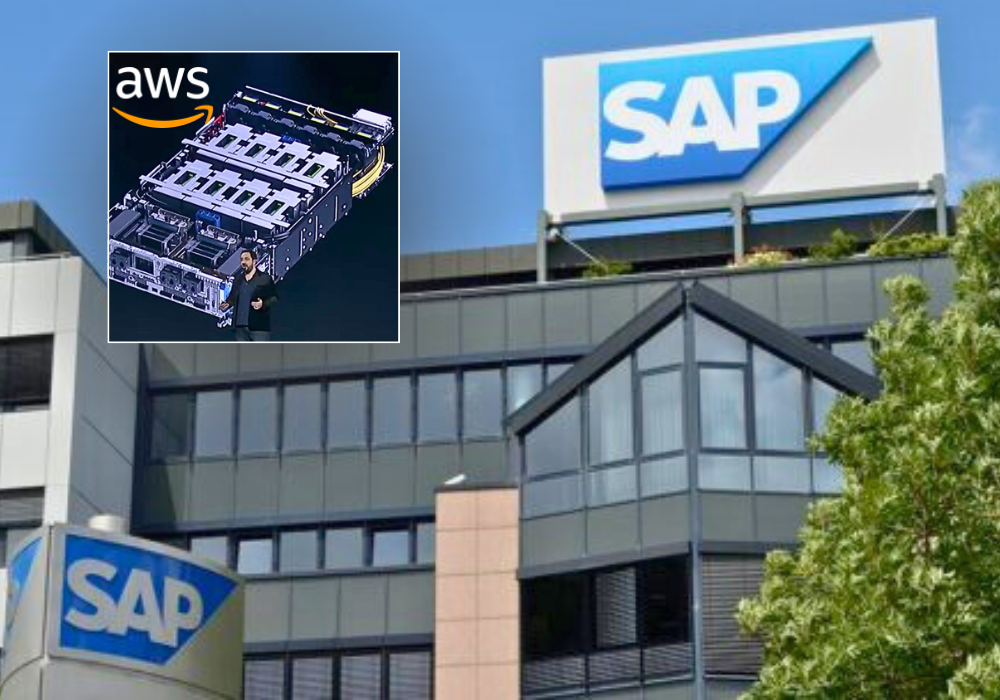
SAP To Use AWS's AI Chips and Integrate GenAI Models from Amazon Bedrock

SAP To Use AWS's AI Chips and Integrate GenAI Model from Amazon Bedrock

Amazon Web Services (AWS) and SAP SE have announced an expanded strategic collaboration to enhance cloud enterprise resource planning (ERP) experiences and enable enterprises to harness generative artificial intelligence (AI) for new capabilities and efficiencies. This partnership aims to transform how businesses operate by integrating generative AI into their core processes.

SAP plans to utilize AWS's specialized chips for training and deploying its future Business AI offerings. The chips in question are AWS Trainium and AWS Inferentia, which are purpose-built for artificial intelligence (AI) and machine learning (ML) workloads. This move is part of the broader strategic collaboration between AWS and SAP to integrate generative AI into SAP's cloud enterprise resource planning (ERP) experiences.

AWS Trainium and AWS Inferentia are custom-built chips designed by Amazon Web Services (AWS) for specific machine learning (ML) tasks. AWS Trainium is optimized for deep learning (DL) training of large models, including generative Al models.

Each Trainium accelerator includes two second-generation NeuronCores and 32 GB of high- bandwidth memory, delivering up to 190 TFLOPS of FP16/BF16 compute power, ideal for training tasks in natural language processing, computer vision, and recommendation systems. While Inferentia2 accelerators have 32 GB of HBM per accelerator, significantly increasing memory capacity and bandwidth.

By leveraging AWS's powerful hardware, SAP aims to enhance the performance and efficiency of its AI-driven business applications. This will enable SAP customers to harness the capabilities of generative AI for a variety of applications, streamlining processes and driving innovation within their operations.

In addition, the collaboration also includes the integration of generative AI models from Amazon Bedrock, such as the Anthropic Claude 3 model family and Amazon Titan, into the SAP AI Core infrastructure. This will provide SAP customers with access to high-performing large language models (LLMs) and other foundation models (FMs) that can be customized with their own data.

Amazon Bedrock is a fully managed service provided by Amazon Web Services (AWS) that enables developers to build and scale generative Al applications using foundation models (FMs).

The goal is to make it easier for customers to adopt the RISE with SAP solution on AWS, improve the performance of SAP workloads in the cloud, and embed generative AI across an enterprise's portfolio of business-critical applications. This initiative is expected to accelerate the adoption of generative AI and modernize key business processes built on SAP solutions.

The generative AI hub in SAP AI Core infrastructure provides customers with secure access to a broad range of large language models (LLMs) that can easily be integrated into SAP business applications. Tens of thousands of customers use Amazon Bedrock to easily, quickly and securely build and scale generative AI applications using FMs from leading AI companies such as AI21 Labs, Anthropic, Cohere, Meta, Mistral AI, Stability AI and Amazon.

Intel Says Its Gaudi 2 Accelerator is Nvidia H100's Only Benchmarked Alternative for Generative AI

Intel Says Its Gaudi 2 Accelerator is Nvidia H100's Only Benchmarked Alternative for Generative AI

Intel Gaudi 2 continues to shine as the sole benchmarked alternative to Nvidia's H100 in the realm of generative AI (GenAI) performance. Intel's ambitious goal to deliver competitive AI solutions across its portfolio is evident through the latest MLPerf v4.0 benchmark results. "The Intel Gaudi 2 AI accelerator remains the only benchmarked alternative to Nvidia H100 for generative AI (GenAI) performance and provides strong performance-per-dollar," said Intel, in an official news release. 

In a recent MLPerf GPT-J inference benchmark, Intel's Gaudi 2 achieved near-parity performance with Nvidia's H100, reinforcing its position as a formidable alternative.

The Intel® Gaudi® 2 accelerator is a heavyweight contender in the AI accelerator arena, designed specifically for deep learning training and inference. It delivers two times the performance of A100 on Computer Vision, NLP, and large scale models.

Gaudi 2 shrinks the process from 16nm to 7nm, increases the number of Al-customized Tensor Processor Cores from 8 to 24, adds FP8 support, and integrates a media compression engine.

Additionally, Intel remains the exclusive server CPU vendor to submit MLPerf results. The 5th Gen Intel Xeon processors have shown an impressive 1.42x improvement compared to their 4th Gen counterparts in MLPerf Inference v3.1.

Intel Says Its Gaudi 2 Accelerator is Nvidia H100's Only Benchmarked Alternative for Generative AI
Intel Gaudi 2 

Developed by Habana Labs, now part of Intel, the Gaudi 2 is equipped with a whopping 96GB of HBM2E memory offering ample space to store and process massive datasets. Additionally, the high bandwidth of 2.45 TB/s ensures smooth data flow during training and inference processes, minimizing bottlenecks.

Habana Labs is considered the center of excellence for AI solutions at Intel, and Intel acquired the company in 2019 for approximately $2 billion.

It is said that Habana Labs is now working on Gaudi 3, which is expected to offer a significant performance boost.

Intel Gaudi 2 Vs NVIDIA H100 / A100

Gaudi 2 vs. NVIDIA H100

Performance: Gaudi 2 remains the only benchmarked alternative to Nvidia H100 for generative AI (GenAI) performance.

Price-to-Performance: It provides strong performance-per-dollar.

MLPerf Results: Intel is the exclusive server CPU vendor to submit MLPerf results, showcasing Gaudi 2's capabilities.

Scalability: Gaudi 2 integrates 24 100-gigabit RDMA over Converged Ethernet (RoCE2) ports, making it cost-effective and easy to scale out training capacity.

Networking: These ports enable efficient communication within the server, enhancing throughput.

Intel Gaudi 2 vs. NVIDIA A100

Inference: Gaudi 2 matches the latency of Nvidia H100 systems on decoding and outperforms the Nvidia A100 in large language model (LLM) inference.

Performance: Gaudi 2 is about twice faster than the NVIDIA A100 80GB for both training and inference. 

Available on the Intel Developer Cloud for easy access.

Memory Bandwidth: Gaudi 2 achieves higher memory bandwidth utilization than H100 and A100.

In summary, Intel Gaudi 2 offers compelling performance-per-dollar and can be a respected alternative to Nvidia's offerings. While Nvidia A100 remains a powerhouse, Gaudi 2 provides better value in many scenarios.

Nvidia Unveils World's Most Powerful Chip for AI

Nvidia Unveils World's Most Powerful Chip for AI

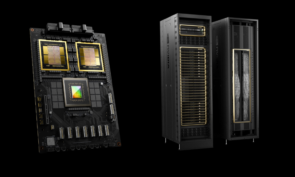
NVIDIA has recently announced the Blackwell platform, which includes the Blackwell B200 GPU, described as the world's most powerful chip for AI. The Blackwell GPU architecture is designed to enable organizations to build and run real-time generative AI on trillion-parameter large language models with significantly reduced cost and energy consumption.

The B200 GPU boasts up to 20 petaflops of FP4 horsepower from its 208 billion transistors. This advancement is expected to have a wide impact across various industries, including data processing, engineering simulation, electronic design automation, computer-aided drug design, and quantum computing.

NVIDIA also announced the NVIDIA Blackwell platform that would let organizations everywhere to build and run real-time generative AI on trillion-parameter large language models at up to 25x less cost and energy consumption than its predecessor.

The Blackwell GPU architecture features six transformative technologies for accelerated computing, which will help unlock breakthroughs in data processing, engineering simulation, electronic design automation, computer-aided drug design, quantum computing and generative AI — all emerging industry opportunities for NVIDIA.

“For three decades we’ve pursued accelerated computing, with the goal of enabling transformative breakthroughs like deep learning and AI,” said Jensen Huang, founder and CEO of NVIDIA. “Generative AI is the defining technology of our time. Blackwell is the engine to power this new industrial revolution. Working with the most dynamic companies in the world, we will realize the promise of AI for every industry.”

Blackwell Innovations to Fuel Accelerated Computing and Generative AI

Nvidia Unveils World's Most Powerful Chip for AI

Blackwell’s six revolutionary technologies, which together enable AI training and real-time LLM inference for models scaling up to 10 trillion parameters, include:
  • World’s Most Powerful Chip — Packed with 208 billion transistors, Blackwell-architecture GPUs are manufactured using a custom-built 4NP TSMC process with two-reticle limit GPU dies connected by 10 TB/second chip-to-chip link into a single, unified GPU.
  • Second-Generation Transformer Engine — Fueled by new micro-tensor scaling support and NVIDIA’s advanced dynamic range management algorithms integrated into NVIDIA TensorRT™-LLM and NeMo Megatron frameworks, Blackwell will support double the compute and model sizes with new 4-bit floating point AI inference capabilities.
  • Fifth-Generation NVLink — To accelerate performance for multitrillion-parameter and mixture-of-experts AI models, the latest iteration of NVIDIA NVLink® delivers groundbreaking 1.8TB/s bidirectional throughput per GPU, ensuring seamless high-speed communication among up to 576 GPUs for the most complex LLMs.
  • RAS Engine — Blackwell-powered GPUs include a dedicated engine for reliability, availability and serviceability. Additionally, the Blackwell architecture adds capabilities at the chip level to utilize AI-based preventative maintenance to run diagnostics and forecast reliability issues. This maximizes system uptime and improves resiliency for massive-scale AI deployments to run uninterrupted for weeks or even months at a time and to reduce operating costs.
  • Secure AI — Advanced confidential computing capabilities protect AI models and customer data without compromising performance, with support for new native interface encryption protocols, which are critical for privacy-sensitive industries like healthcare and financial services.
  • Decompression Engine — A dedicated decompression engine supports the latest formats, accelerating database queries to deliver the highest performance in data analytics and data science. In the coming years, data processing, on which companies spend tens of billions of dollars annually, will be increasingly GPU-accelerated.

OpenAI To Buy $51 Mn of AI Chips from OpenAI's CEO backed Startup

OpenAI To Buy $51 Mn of AI Chips from OpenAI's CEO backed Startup

ChatGPT maker OpenAI, in 2019, had signed a nonbinding agreement to spend $51 million on AI chips from a startup called Rain AI into which OpenAI CEO has invested in his personal capacity.

According to a report by Wired, Altman had personally invested by more than $1 million into Rain AI, by leading a seed round in the startup in July 2020. The letter of intent has not been previously reported. The AI Chip Startup is located less than a mile from OpenAI’s headquarters in San Francisco.

Founded in 2017, by Gordon Wilson, Jack Kendall and Juan Nino, Rain AI is working on a chip it calls a neuromorphic processing unit, or NPU, designed to replicate features of the human brain. The Sam Altman backed startup claims that its brain-inspired NPUs will yield potentially 100 times more computing power and, for training, 10,000 times greater energy efficiency than GPUs, primarily sourced from Nvidia.

Just a few days back, Biden-led US administration had reportedly forced a Saudi Aramco-backed venture capital firm Prosperity7, to sell its shares in Rain AI, reported Bloomberg.

Rain AI had also raised a small seed funding from the venture unit of Chinese search engine Baidu.

While Amazon and Google have spent years developing their own custom chips for AI projects. Altman has refused to rule out OpenAI making its own chips apparently because of the fact that unlike OpenAI Amazon and Google have other business verticals–revenues to fund the AI chip of their own.

Intel Launches New Core 14th Gen Desktop Processors with AI Overclocking

Intel Launches New Core 14th Gen Desktop Processors with AI Overclocking

Intel today announced the launch of the new Intel® Core™ 14th Generation desktop processor family, led by the Intel® Core™ i9-14900K. This latest-generation desktop processor family includes six new unlocked desktop processors at launch, delivering up to 24 cores and 32 threads and up to 6 GHz of frequency right out of the box. 

Additionally, the Intel® Core™ i7-14700K arrives with 20 cores and 28 threads as it has four more Efficient-cores (E-cores) compared with the prior generation. And Intel’s Extreme Tuning Utility (XTU) now features the new AI Assist feature, bringing one-click AI-guided overclocking to select unlocked Intel Core 14th Gen desktop processors. Notably, as of October 2023, AI Assist is supported on certain Intel Core 14th gen unlocked SKUs.

Roger Chandler, Intel vice president and general manager, Enthusiast PC and Workstation​, Client Computing Group, said, "Since the introduction of our performance hybrid architecture, Intel has consistently raised the bar for desktop performance. With our Intel Core 14th Generation processors, we’re showing once again why enthusiasts turn to Intel for the best desktop experience available on the market today."

With faster clock speeds up and down the processor stack – led by the flagship i9-14900K’s 6 GHz turbo frequencies – the Intel Core 14th Gen desktop processor family powers the world’s best desktop experience for enthusiasts.


Connectivity

Support for Wi-Fi 6/6E, Bluetooth 5.3, Wi-Fi 7, and Thunderbolt 4, along with compatibility with 600/700-series chipsets for easy upgrades.

Gaming Performance

Intel claims that the new Core 14th Gen processors power an immersive gaming experience with up to 23% gaming performance uplift compared to leading competitor processors, while new gaming-focused features like Intel® Application Optimization (APO) ensure better-than-ever application threading alongside existing Intel® Thread Director application thread scheduling.

Intel® Application Optimization is a policy within Intel® Dynamic Tuning Technology that optimizes performance on select games, with the required configurations on select Intel Core 14th Gen processors.

AI Guided Overclocking

Intel Core 14th Gen unlocked processors continue to offer an unparalleled overclocking experience for everyone – from experts to beginners. Latest-generation unlocked desktop processors now include the new Intel® XTU AI Assist feature for AI guided overclocking, as well as support for DDR5 XMP speeds well beyond 8,000 megatransfers/second (MT/S).

Intel Core 14th Gen desktop processors remain compatible with both Intel 600 and 700 series chipsets, giving enthusiasts the ability to easily upgrade their existing systems and enjoy latest-generation gaming and creator performance.

Intel Core 14th Gen desktop processors will be available at retail outlets and via OEM partner systems starting Oct. 17, 2023.

In A 1st, NVIDIA To Become $1 Trillion Company

In A 1st, NVIDIA To Become $1 Trillion Company

In a what can be seen as an overnight event, American chipmaker Nvidia could soon land a spot in the most elite club of $1 Trillion companies, joining Apple, Microsoft, Alphabet and Amazon. With this, Nvidia will be first chipmaker to become $1 Trillion Company. 

The chipmaker saw its shares surge 27% on Thursday, bringing its market value to just under the $1 trillion mark at about $974 billion. It was $755 billion at Wednesday’s close.

Shares in Nvidia rose 23% on Thursday morning in New York after its sales forecast came in more than 50% ahead of Wall Street's previous estimates.

Nvidia added some $170bn to its market value following Wednesday's quarterly report. That is more than the entire value of Intel or Qualcomm and the biggest one-day gain ever for a US stock, according to figures from Bloomberg.

The surge in Nvidia shares was bolstered by the chipmaker's claim to be the only company whose tech is capable of meeting demand from across the industry to build generative AI, systems capable of creating human-like content.

The company said it was raising production of its chips to meet surging demand.

Nvidia’s latest flagship AI Chip — H100, succeeding the A100 chip, is about a $10,000 chip that’s been called the “workhorse” for AI applications.

This H100 AI chip is being used by developers to build large language models (LLMs), which are at the heart of AI applications like OpenAI’s ChatGPT. Running these systems is expensive and requires powerful computers to churn through terabytes of data for days or weeks at a time. They also rely on hefty computing power so the AI model can generate text, images or predictions.

In March this year, the company introduced NVIDIA AI Foundations to help businesses create and operate custom large language models and generative AI models trained with their own proprietary data for domain-specific tasks.

The computer industry is going through two simultaneous transitions — accelerated computing and generative AI,” said Jensen Huang, founder and CEO of NVIDIA, in a company press release.

A trillion dollars of installed global data center infrastructure will transition from general purpose to accelerated computing as companies race to apply generative AI into every product, service and business process.

Our entire data center family of products — H100, Grace CPU, Grace Hopper Superchip, NVLink, Quantum 400 InfiniBand and BlueField-3 DPU — is in production. We are significantly increasing our supply to meet surging demand for them,” he said.

During the first quarter of fiscal 2024, NVIDIA returned to shareholders $99 million in cash dividends.

Market Reports

Market Report & Surveys
IndianWeb2.com © all rights reserved