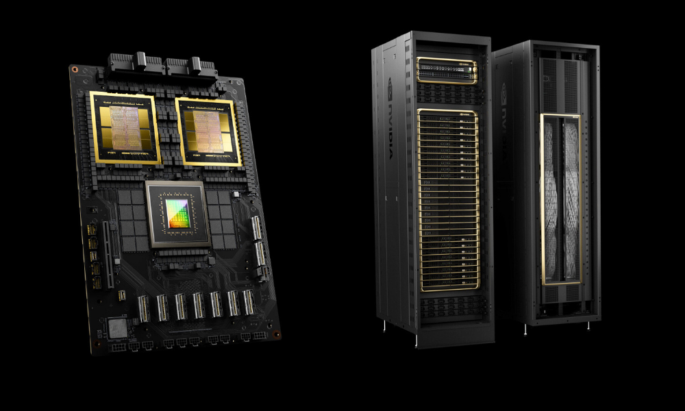
The B200 GPU boasts up to 20 petaflops of FP4 horsepower from its 208 billion transistors. This advancement is expected to have a wide impact across various industries, including data processing, engineering simulation, electronic design automation, computer-aided drug design, and quantum computing.
NVIDIA also announced the NVIDIA Blackwell platform that would let organizations everywhere to build and run real-time generative AI on trillion-parameter large language models at up to 25x less cost and energy consumption than its predecessor.
The Blackwell GPU architecture features six transformative technologies for accelerated computing, which will help unlock breakthroughs in data processing, engineering simulation, electronic design automation, computer-aided drug design, quantum computing and generative AI — all emerging industry opportunities for NVIDIA.
“For three decades we’ve pursued accelerated computing, with the goal of enabling transformative breakthroughs like deep learning and AI,” said Jensen Huang, founder and CEO of NVIDIA. “Generative AI is the defining technology of our time. Blackwell is the engine to power this new industrial revolution. Working with the most dynamic companies in the world, we will realize the promise of AI for every industry.”
Blackwell Innovations to Fuel Accelerated Computing and Generative AI
 |
Blackwell’s six revolutionary technologies, which together enable AI training and real-time LLM inference for models scaling up to 10 trillion parameters, include:
- World’s Most Powerful Chip — Packed with 208 billion transistors, Blackwell-architecture GPUs are manufactured using a custom-built 4NP TSMC process with two-reticle limit GPU dies connected by 10 TB/second chip-to-chip link into a single, unified GPU.
- Second-Generation Transformer Engine — Fueled by new micro-tensor scaling support and NVIDIA’s advanced dynamic range management algorithms integrated into NVIDIA TensorRT™-LLM and NeMo Megatron frameworks, Blackwell will support double the compute and model sizes with new 4-bit floating point AI inference capabilities.
- Fifth-Generation NVLink — To accelerate performance for multitrillion-parameter and mixture-of-experts AI models, the latest iteration of NVIDIA NVLink® delivers groundbreaking 1.8TB/s bidirectional throughput per GPU, ensuring seamless high-speed communication among up to 576 GPUs for the most complex LLMs.
- RAS Engine — Blackwell-powered GPUs include a dedicated engine for reliability, availability and serviceability. Additionally, the Blackwell architecture adds capabilities at the chip level to utilize AI-based preventative maintenance to run diagnostics and forecast reliability issues. This maximizes system uptime and improves resiliency for massive-scale AI deployments to run uninterrupted for weeks or even months at a time and to reduce operating costs.
- Secure AI — Advanced confidential computing capabilities protect AI models and customer data without compromising performance, with support for new native interface encryption protocols, which are critical for privacy-sensitive industries like healthcare and financial services.
- Decompression Engine — A dedicated decompression engine supports the latest formats, accelerating database queries to deliver the highest performance in data analytics and data science. In the coming years, data processing, on which companies spend tens of billions of dollars annually, will be increasingly GPU-accelerated.


 IndianWeb2.com is an independent digital media platform for business, entrepreneurship, science, technology, startups, gadgets and climate change news & reviews.
No comments
Post a Comment