‏إظهار الرسائل ذات التسميات Seminconductor. إظهار كافة الرسائل

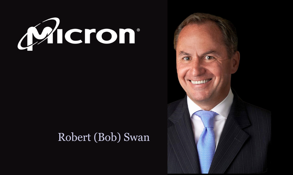
Micron Appoints Robert Swan, Partner at Andreessen Horowitz, To Its Board of Directors

Micron Appoints Robert Swan, Partner at Andreessen Horowitz, To Its Board of Directors

Micron Technology, Inc. (Nasdaq: MU), an industry leader in innovative memory and storage solutions, on Monday, announced the appointment of Robert (Bob) Swan to its board of directors. Swan is currently an operating partner at Andreessen Horowitz (also known as a16z), a venture-capital firm. He will also serve on both the Audit and Finance Committees.

Swan’s extensive background includes his tenure as CFO and later CEO of Intel Corporation, where he oversaw 110,000 employees and $78B in annual sales. Prior to joining Intel, as CFO of eBay, Swan played a significant role in driving the company’s global expansion strategy. Swan also held notable roles as CFO at Electronic Data Systems Corp., TRW Inc., and Webvan Group, Inc., where he additionally served as COO and CEO.

Bob’s track record in driving growth and operational excellence at some of the world’s leading technology companies will be invaluable to Micron as we continue to scale our business and solidify our position at the forefront of the memory and storage industry,” said Micron President and CEO Sanjay Mehrotra. “We are thrilled to welcome Bob to our board and look forward to his contributions to our strategic direction and long-term success.”

In addition to his new position at Micron, Swan is on the boards of several organizations, including the board of directors for Nike, Inc., Flexport and the board of commissioners of GoTo Group. He previously served on the board of directors for eBay, Applied Materials, Intel and Skype.

Bob’s proven ability to navigate complex market dynamics and foster innovation will be pivotal for Micron as we advance our strategic objectives and uphold our commitment to delivering state-of-the-art memory and storage solutions,” said Robert E. Switz, chairman of the board at Micron.We are eager to collaborate with Bob and benefit from his vision, financial acumen and leadership experience.

Swan began his career at General Electric, where he spent 15 years in numerous senior finance roles, including divisional CFO for GE Transportation Systems, GE Healthcare Europe, and GE Lighting. Swan received his B.S. from the University at Buffalo and his M.B.A. from the State University of New York at Binghamton. He received his honorary doctorate from Binghamton in 2022.

About Micron Technology, Inc.

We are an industry leader in innovative memory and storage solutions transforming how the world uses information to enrich life for all. With a relentless focus on our customers, technology leadership, and manufacturing and operational excellence, Micron delivers a rich portfolio of high-performance DRAM, NAND and NOR memory and storage products through our Micron® and Crucial® brands. Every day, the innovations that our people create fuel the data economy, enabling advances in artificial intelligence and 5G applications that unleash opportunities — from the data center to the intelligent edge and across the client and mobile user experience. To learn more about Micron Technology, Inc. (Nasdaq: MU), visit micron.com.

Tata Group to Build the Nation’s 1st Indigenous Semiconductor Assembly and Test Facility in Assam

Tata Group to Build the Nation’s 1st Indigenous Semiconductor Assembly and Test Facility in Assam

INR 27,000 crore investment in a greenfield facility in Assam for assembly and testing of semiconductor chips for applications across automotive, mobile devices, artificial intelligence (AI), and other key segments to serve customers globally.

In a significant step towards creating an end-to-end semiconductor manufacturing ecosystem in India, Government of India has approved a proposal by Tata Electronics to build a state-of-the-art, greenfield semiconductor assembly and test facility in Jagiroad, Assam. The facility will be built with an investment outlay of INR 27,000 crore and is expected to generate over 27,000 direct and indirect jobs in the region.

Tata Electronics Pvt Ltd (wholly owned subsidiary of Tata Sons Pvt Ltd) will build this facility focusing on three key platform technologies - Wire Bond, Flip Chip, and a differentiated offering called Integrated Systems Packaging (ISP), with plans of expanding the roadmap to advanced packaging technologies in the future. These technologies are extremely critical for key applications in India – like automotive (especially electric vehicles), communications, network infrastructure and others.

Tata Electronics has already made significant investments in indigenous technology development for all these platforms and has put together a very credible team with over 1,000+ years of global domain experience to drive this project. The proposed facility will serve the growing global demands across key market segments like AI, industrial, and consumer electronics.

The construction of the facility is scheduled to start this year with the first phase of the facility becoming operational by mid-2025 and will provide an immense boost to industrialization in North-East India. The project is envisioned under the Government of India’s Semiconductor policy being driven by the India Semiconductor Mission and the Government of Assam’s Electronics policy.

Semiconductor assembly and test is a critical part of the semiconductor value chain where wafers manufactured by semiconductor fabs are assembled or packaged and then tested before they are finally used in the desired product. Innovations in semiconductor assembly and test are driving increased performance, reduced form factor, and reduced costs of semiconductor chips.

Commenting on the announcement, N Chandrasekaran, Chairman, Tata Sons said, “We are in a unique time for the electronics manufacturing market globally and the world is seeking a more secure and resilient electronics supply chain. With our announcement of the semiconductor fab and this strategic project in semiconductor assembly and test, we will be enabling our global customers to base a key part of their semiconductor value chain in India. Alongside mitigating global supply chain risks, I am confident that this project will have a transformational impact towards technology led industrialization and job creation in the Northeast in particular.

Under the decisive leadership of Hon’ble Prime Minister Shri Narendra Modi, the Government of India has developed a comprehensive central and state semiconductor policy. This along with support from Ministry of Electronics and Information Technology, India Semiconductor Mission and the Government of Assam has made this announcement possible.”

Dr Randhir Thakur, CEO & MD, Tata Electronics said, “The strategy of serving across the semiconductor value chain is our differentiator and will enable Tata Electronics to deliver complete system offerings to customers. We have a critical window of opportunity where we see tremendous customer pull from global players for manufacturing in India and we plan to capitalize on this opportunity and leapfrog through technology innovation. This investment will go a long way in putting India on the map of global semiconductor manufacturing and in spurring a complete domestic ecosystem for high technology manufacturing while being an enabler for the indigenous product ecosystem.”

The proposed facility in Jagiroad is strategically located with access to abundant water and green power – a key sustainability consideration for the Tata group and its customers globally. Assam is also closer to the current semiconductor packaging & test hubs in countries like Taiwan, Malaysia, Vietnam, and Singapore. Assam has technical and engineering workforce available from the entire North-East India, providing a stable talent pool for this project as well as the ecosystem development that this project will seed. This new initiative from Tata Electronics will bring to India a portfolio of cutting-edge semiconductor technologies, advanced skill set and talent, and a network of semiconductor manufacturing suppliers and ecosystem partners, resulting in foundational development of indigenous semiconductor ecosystem in India. This Assembly & Test facility will be able to directly ship semiconductor chips to end-users and OEMs (Original Equipment Manufacturers) in India and the world.

About the Tata group

Founded by Jamsetji Tata in 1868, the Tata group is a global enterprise, headquartered in India, comprising 30 companies across ten verticals. The group operates in more than 100 countries across six continents, with a mission ‘To improve the quality of life of the communities we serve globally, through long-term stakeholder value creation based on Leadership with Trust’.

Tata Sons is the principal investment holding company and promoter of Tata companies. Sixty-six percent of the equity share capital of Tata Sons is held by philanthropic trusts, which support education, health, livelihood generation and art and culture.

In 2022-23, the revenue of Tata companies, taken together, was $150 billion (INR 12 trillion). These companies collectively employ over 1 million people. Each Tata company or enterprise operates independently under the guidance and supervision of its own board of directors. There are 29 publicly listed Tata enterprises with a combined market capitalization of $350 billion as of February 2024.

About Tata Electronics

Tata Electronics is a global player in the electronics manufacturing business with fast emerging capabilities in Electronics Manufacturing Services, Semiconductor Assembly & Test, Semiconductor Foundry, and Design Services. Founded in 2020 as a greenfield venture of the Tata group, the company aims to better serve global customers through integrated offerings across a trusted electronics and semiconductor value chain. With a fast-expanding workforce, the company presently employs over 15,000 people and has facilities in Tamil Nadu and Karnataka in India. Tata Electronics also aims to work towards creating a conscientious socio-economic footprint by employing large number of women in its workforce and providing necessary assistance to local communities in health, hygiene, and education.

Siemens, sureCore and Semiwise to Develop Quantum Computer Ready Cryogenic Semiconductor Designs for Extreme Cold Conditions

Siemens, sureCore and Semiwise to Develop Quantum Computer Ready Cryogenic Semiconductor Designs for Extreme Cold Conditions

Collaboration between Siemens, sureCore and Semiwise to develop cryogenic semiconductor designs capable of operating in extreme cold conditions required for quantum computing

Siemens Digital Industries Software, a business unit of Siemens, has announced its collaboration with sureCore and Semiwise to develop groundbreaking cryogenic CMOS circuits capable of operating at temperatures near absolute zero – a fundamental component of quantum computing systems. The joint effort holds the potential for dramatic advances in both performance and power efficiency for next-generation integrated circuits (IC) targeting quantum computing – considered the leading edge in the high-performance computing (HPC) research and development.

The key to unlocking the potential of quantum computing for HPC and other fast-growing applications lies in the availability of control electronics capable of operating at cryogenic temperatures. Using advanced analog/mixed-signal IC design technology from Siemens, Semiwise has developed cryogenic CMOS circuit designs featuring cryogenic SPICE models as well as SPICE simulator technology that can perform accurate analyses at cryogenic temperatures.

Semiwise is providing this intellectual property (IP), developed using Siemens’ Analog FastSPICE (AFS), to sureCore for the development of sureCore’s revolutionary line of CryoIP, which aims to enable the design of CryoCMOS control chips seen as crucial for unlocking the commercial potential for quantum computing.

In the development of its CryoIP product line, sureCore also used Siemens’s Analog FastSPICE platform and Siemens’ Solido™ Design Environment software, both of which demonstrated reliable and accurate operation at cryogenic temperatures, empowering sureCore to construct analog circuits, standard cell libraries, and memory designs including SRAM, register files, and ROM, using Semiwise’s cryogenic transistor models. Further, Siemens’ Analog FastSPICE software showcased exceptional capabilities in handling foundry device models at cryogenic conditions, helping deliver efficient analog, mixed-signal, and digital circuit design and verification functionality without convergence issues. The result is a high level of accuracy and performance, setting the stage for potentially groundbreaking advancements in quantum computing.

sureCore is rapidly progressing towards its first CryoIP tapeout, leveraging GlobalFoundries' 22FDX® PDK.

Paul Wells, CEO of sureCore, underscored the pivotal role of this partnership. "The critical storage element and the bit cell must essentially be treated as an analog circuit that is highly sensitive to process variability and mismatch,” said Wells. “When we develop new memory designs and their associated compilers, we need to run thousands of statistical circuit simulations to guarantee the yield and reliability of our IP. Our partnership with Siemens EDA has enabled us to leverage Siemens' Custom IC verification technology to build robust cryogenic IP cores, specifically tailored for Quantum applications."

"This partnership symbolizes Siemens' unwavering dedication to advancing the quantum computing domain,” said Amit Gupta, general manager and vice president of the Custom IC Verification Division, Siemens Digital Industries Software. The groundbreaking technologies and solutions developed have the potential to redefine the boundaries of high-performance computing."

Siemens' Analog FastSPICE platform, powered by technology from Siemens’ Analog FastSPICE eXTreme™ platform, offers cutting-edge circuit verification for nanometer analog, radio frequency (RF), mixed-signal, memory, and custom digital circuits. It holds foundry certifications across all major foundries and is qualified across various process nodes, from mature to the most advanced. Siemens' Analog FastSPICE platform offers a comprehensive use model, including small signal, transient, RF, noise, aging, and multi-sim verification capabilities, with drop-in compatibility with industry-standard SPICE-based flows. This all-encompassing solution boasts high performance, capacity, and flexible features.

Siemens' Solido Design Environment plays a pivotal role by providing a comprehensive cockpit for nominal and variation-aware analysis and encompasses SPICE-level circuit simulation setup, measurements, regressions, waveforms, and statistical results analysis. Powered by AI technology, Solido Design Environment assists users in identifying optimization paths to improve circuit power, performance, and area - facilitating production-accurate statistical yield analysis, reducing runtime compared to brute-force methods.

Siemens Digital Industries Software helps organizations of all sizes digitally transform using software, hardware and services from the Siemens Xcelerator business platform. Siemens' software and the comprehensive digital twin enable companies to optimize their design, engineering and manufacturing processes to turn today's ideas into the sustainable products of the future. From chips to entire systems, from product to process, across all industries. Siemens Digital Industries Software – Accelerating transformation.

Note: A list of relevant Siemens trademarks can be found here. Other trademarks belong to their respective owners. sureCore, SureFIT and When low power is paramount are trademarks of sureCore Limited. Other trademarks belong to their respective owners. 

Market Reports

Market Report & Surveys
IndianWeb2.com © all rights reserved