Showing posts with label Semiconductor Startups. Show all posts

IAN Alpha Fund Leads $6 Mn Investment Round in BigEndian Semiconductors

  • As AI and edge computing surge, startup bets on security-first chip design to position India as a product-led semiconductor hub
IAN Group, the country’s largest early-stage investment platform, has led a USD$ 6 million funding round in BigEndian, through IAN Alpha Fund, the second in its series of VC funds, along with Vertex Ventures SEA, IvyCap Ventures, and other angel investors.

Sunil Kumar, Co-Founder & CEO, BigEndian Semiconductors
Sunil Kumar
The fresh capital will be deployed across chip design, team expansion, and tapeout cycles, one of the most capital-intensive and critical stages in semiconductor development. The company is also building cross-border partnerships, particularly in Taiwan, to bridge design and manufacturing, an essential step in navigating today’s globally distributed semiconductor supply chain.

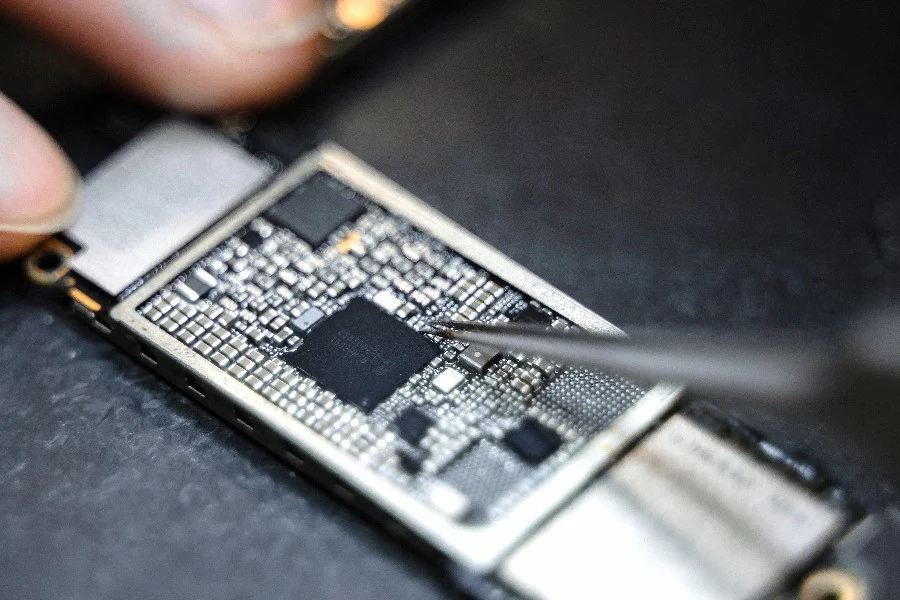
Founded in 2024, BigEndian is developing System-on-Chips (SoCs) focused on AI Vision applications that enable machines to process and interpret visual data instantly. These are critical for applications such as smart surveillance, autonomous systems, industrial automation, and connected devices, where decisions need to be made at the edge, not the cloud.

The opportunity is also being shaped by a structural shift in the market. A significant majority of India’s surveillance and CCTV infrastructure currently relies on imported, predominantly Chinese SoCs. With increasing regulatory scrutiny globally and India’s STQC norms pushing for trusted, non-Chinese alternatives, OEMs are actively seeking reliable indigenous solutions, creating a well-defined and time-sensitive gap that companies like BigEndian are positioned to address.

The semiconductor industry is undergoing a structural shift away from general-purpose chips toward highly specialized silicon designed for AI, edge computing, and real-time data processing. At the same time, rising concerns around data security, cyber threats, and digital sovereignty are forcing companies and governments to rethink how chips are designed at the most fundamental level.

It is at this intersection that BigEndian is building, with a full-stack approach that integrates hardware, security, and software. Its “Secure by Design™” philosophy embeds security at the silicon level rather than as an afterthought, while its platform-led approach is designed to enable long-term ecosystem integration and recurring value creation.

Sunil Kumar, Co-Founder & CEO, BigEndian Semiconductors, said, “Raising capital in semiconductors is never about the money alone. It’s about earning trust in your ability to execute. This funding validates not just our technology, but our approach to building silicon the hard way: from architecture to tape-out, with a long-term roadmap in mind. India has no shortage of engineering talent or market demand. What we need is conviction capital that understands the cost, risk, and importance of building fabless semiconductor companies. At BigEndian, we’re committed to proving that world-class chips can be designed, built, and scaled from India.”

Rajnish Kapur, Managing Partner, IAN Alpha Fund, said, “The semiconductor landscape is moving from scale to specialization, with increasing emphasis on secure, domain-specific chip design. BigEndian is building at the intersection of AI, edge computing, and hardware-level security, but what stood out for us, at IAN, was the team’s proven execution capability, with prior successful tape-outs, and the early market validation they have demonstrated through OEM partnerships.

We believe India’s opportunity in semiconductors lies not just in design services, but in building globally competitive product companies. BigEndian’s full-stack approach and focus on trusted, indigenous solutions position it well to address a critical and evolving market need.”

India’s opportunity in this space is both clear and urgent. The country already contributes significantly to global semiconductor design talent, yet captures limited value due to the absence of large-scale product companies. With policy tailwinds such as the India Semiconductor Mission and growing investor appetite for deeptech, the ecosystem is now primed for companies that can move up the value chain.

The broader market tailwinds are hard to ignore. AI-driven workloads, proliferation of smart devices, and the rise of edge computing are driving demand for custom silicon at an unprecedented pace. At the same time, geopolitical shifts and supply chain disruptions have made semiconductor self-reliance a strategic priority for nations.

Early indicators of market traction further strengthen this outlook, with the company already engaging with OEM partners who are actively aligning with emerging regulatory requirements and seeking dependable alternatives in the ecosystem.

In this environment, startups like BigEndian are not just building products, they are helping define India’s role in the global semiconductor value chain.

About BigEndian Semiconductors

BigEndian Semiconductors is a fabless semiconductor startup building secure, high-performance System-on-Chips (SoCs) for AI Vision applications - designed in India for the global. Founded by a veteran team with a track record in delivering world-first innovations—from 4G chipsets to unicorn-scale SaaS platforms—BigEndian is focused on developing silicon platforms that power next-generation AI Vision systems powering surveillance, industrial, automotive, IoT, and enterprise systems.

At the heart of BigEndian’s vision is a “Secure by Design™” philosophy that tightly integrates hardware and software. With deep expertise in VLSI, system architecture, and embedded software, the company is developing trusted silicon solutions that serve both national security and commercial needs.

Headquartered in Bengaluru with strategic partnerships across Taiwan and India, BigEndian is working to build an ecosystem that supports end-to-end semiconductor innovation—from architecture to tapeout to product launch. The company is backed by a leadership team with decades of experience at Intel, ARM, Broadcom, Cypress, Centillium, and Zenoti, and is supported by government programs and deep-tech investors.

BigEndian is on a mission to help India become a global hub for semiconductor design, innovation, and manufacturing, starting with Fabless, and building toward Fab.

About IAN Alpha Fund

IAN Alpha Fund, a $100 Mn SEBI-registered Category II AIF VC Fund, is the 2nd fund in IAN Group’s series of funds. The Fund explores opportunities in diverse sectors such as healthtech, cleantech, deep tech, agritech, medtech, hardware and electronics, manufacturing, Web 3.0, Metaverse, Industry 4.0, SaaS, and other sectors where innovation is transformational. The Fund invests in innovative startups solving real problems for India and the world, with sustainable business models enabling scale by leveraging technology. With the IAN Alpha Fund, IAN Group continues its two-decade legacy of building a portfolio of technology-focused, innovative companies led by founders who not only understand customer needs but also have the leadership qualities to build large and valuable businesses.

IAN Group is India’s largest horizontal platform for early-stage investments, comprising the IAN Angel Fund, BioAngels, and a series of SEBI-registered Venture Capital Funds, the latest being a US$100mn VC Fund, IAN Alpha Fund. IAN enables entrepreneurs to raise from Rs. 50 lakhs to Rs. 50 crores, supported by high-quality mentoring by successful entrepreneurs, enabling access to global markets. IAN Group backs founders across domains and helps them scale their companies across India and beyond. Forbes has recognised IAN as one of the most iconic business and economic developments of Independent India over the last 75 years, alongside institutions such as LIC, NASSCOM, the RBI, and Naukri.com.

Raana Semiconductors Secures $3M Seed Funding to Build Indigenous Silicon Ingot Systems

Raana Semiconductors Secures $3M Seed Funding to Build Indigenous Silicon Ingot Systems

Raana Semiconductors Pvt Ltd, a Tamil Nadu-based deep-tech startup, has raised $3 million in a seed funding round led by Equirus Innovatex Fund and Artha Venture Fund, with participation from IvyCap Ventures, PointOne Capital, CIIE Initiatives (IIMA Ventures), and angel investor Garimella Laxminarayana. The funds will accelerate R&D and product development of indigenous silicon ingot growth systems.

Key Highlights of the Funding Round

  • Amount Raised: $3 million (Seed round, pure equity)
  • Lead Investors: Equirus Innovatex Fund, Artha Venture Fund
  • Other Participants: IvyCap Ventures, PointOne Capital, CIIE Initiatives (IIMA Ventures), Garimella Laxminarayana (angel investor)
  • Advisory Partner: Prequate Advisory served as the sole strategic advisor

Company Profile

  • Name: Raana Semiconductors Pvt Ltd (RSPL)
  • Location: Tamil Nadu, India
  • Sector: Deep-tech, semiconductor manufacturing equipment
  • Specialization: Czochralski (CZ)-based crystal growth systems and single-crystal materials
  • Experience: Over a decade in semiconductor technology

Strategic Use of Funds

  • Product Development: Building indigenous Czochralski monocrystalline silicon ingot growers capable of producing 10–12 inch diameter silicon ingots.
  • Applications: Defence, semiconductor, solar, and medical technologies.
  • Roadmap:
    • Short-term: Solar-grade silicon ingots.
    • Long-term: Semiconductor-grade wafers for chip manufacturing.

Why This Matters

  • Reducing Import Dependence: India relies heavily on overseas suppliers for silicon ingot growth systems. RSPL aims to localize this critical technology.
  • Boost to Semiconductor Ecosystem: Aligns with India’s national semiconductor mission to strengthen domestic manufacturing capacity.
  • Cross-Sector Impact: Vital for renewable energy (solar panels), electronics, defence systems, and medical devices.

Quick Comparison: RSPL vs. Global Context

Aspect RSPL (India) Typical Global Players
Funding Stage Seed ($3M) Series A–C, often $50M+
Focus Indigenous CZ ingot growers Advanced wafer fabs, lithography
Market Gap Local equipment manufacturing Mature ecosystems in US, Taiwan, Korea
Strategic Value Reduces import reliance Expands global dominance

SmartSoC and CDAC's ChipIN Team Up to Offer Free Validation and Foundry Support for India’s Semiconductor Startups

SmartSoC and CDAC's ChipIN Team Up to Offer Free Validation and Foundry Support for India’s Semiconductor Startups

SmartSoC Solutions Pvt. Ltd., a leading semiconductor and embedded engineering services company, has announced its collaboration with the ChipIN Center at Centre for Development of Advanced Computing (CDAC) to support India’s Design Linked Incentive (DLI) Programme. Through this initiative, SmartSoC will extend access to its advanced Post-Silicon Validation (PSV) services to DLI-registered startups and MSMEs on a pro-bono basis, while also offering multiple foundry options within the startup ecosystem.

This collaboration aims to address some of the most critical challenges faced by semiconductor startups in India— including access to diverse foundry services and world class backend validation and characterization infrastructure. By bridging these gaps, SmartSoC and CDAC will empower innovators to accelerate the journey from chip design to commercialization, reduce time-to-market, and strengthen their global competitiveness.

Bharath Desareddy, CEO of SmartSoC

We are proud to be chosen as an engineering collaborator providing vital support to chip innovators in India. This is more than business—it’s our mission. We understand the tough journey from design to functional silicon. SmartSoC pledges to be the one-stop partner guiding startups through real-world complexities. Together, we will build a self-reliant India by leading the semiconductor revolution, not just participating in it.” said Bharath Desareddy, CEO of SmartSoC.

SmartSoC is one of the first Indian companies to partner with multiple foundries, aiming to provide startups with more options so they can select the best fit for their unique design needs. The Post-Silicon Validation services offered by SmartSoC allow startups to rigorously test silicon prototypes against functional, performance, and electrical benchmarks, ensuring compliance with international standards before mass production. These essential services, often unattainable for smaller players due to high costs, are being made accessible to help level the playing field, boost startup credibility, and support their journey to success.

This initiative complements SmartSoC’s ongoing contributions to the DLI Scheme, where the company serves as an engineering collaborator providing end-to-end post-silicon validation, SoC design and verification, physical design, embedded software development, and product engineering support. SmartSoC is actively contributing to advancing India's semiconductor research and development landscape and enabling faster commercialization of indigenous technologies.

We are proud to partner with SmartSoC Solutions to provide Post-Silicon Validation services and multiple foundry options to startups under the DLI Scheme. This collaboration reinforces our commitment to empowering Indian startups and MSMEs with world-class semiconductor design infrastructure, accelerating innovation, and strengthening India’s self-reliant semiconductor ecosystem,” said Shri. E Magesh, Director General, CDAC, India.

Providing multiple foundry options and Post-Silicon Validation through partners like SmartSoC ensures startups are able to confidently transition from design to deployable products. By offering complimentary access to expert labs, test infrastructure, and engineering services, initiatives like this reduce both cost and risk, enabling Indian startups to compete globally,” said Dr. SD Sudarsan, Executive Director, CDAC Bangalore Centre.

Aligned with the Government of India’s Semicon India vision and the larger Atmanirbhar Bharat (Self-Reliant India) mission, this collaboration underscores the importance of industry-government partnerships in building a robust innovation ecosystem.

About SmartSoC:

SmartSoC Solutions is a global provider of semiconductor design and embedded engineering services, specializing in turnkey project execution, custom ASIC development, and foundry services. With deep domain expertise and a solutions-driven approach, SmartSoC enables clients to accelerate growth and scale efficiently. Our collaborative, end-to-end approach enables leading semiconductor and system companies to streamline development cycles and bring differentiated silicon solutions to market with precision.

About ChipIN:

ChipIN is an initiative implemented by the Centre for Development of Advanced Computing (C-DAC) under the Design Linked Incentive (DLI) and Chip to Startup (C2S) programes of MeitY, Government of India, aimed at strengthening India’s semiconductor design ecosystem. The ChipIN Centre at CDAC Bangalore is one of the world’s largest and most advanced semiconductor design infrastructure facilities, providing state-of-the-art EDA tools, IPs, prototyping facilities, and high-performance computing (HPC) resources to Indian startups, MSMEs, and academic institutions. This initiative empowers innovators to design and develop complex semiconductor devices in a cost-effective manner. By fostering strong collaboration between industry, academia, and government, ChipIN serves as a national design infrastructure backbone, accelerating innovation, reducing design cycles, and driving indigenous semiconductor development—thereby laying the foundation for a self-reliant and globally competitive semiconductor ecosystem in India.

IISc-backed Morphing Machines Raises ₹38.36 Cr to Build India’s Next-Gen Semiconductor Accelerator

IISc-backed Morphing Machines Raises ₹38.36 Cr to Build India’s Next-Gen Semiconductor Accelerator

Morphing Machines, a Bengaluru-based fabless semiconductor IP company at the Indian Institute of Science (IISc), has raised ₹38.36 crore in a Series A funding round led by IAN Alpha Fund, with participation from Speciale Invest, IvyCap Ventures, and Navam Capital. Existing investors from the Seed round include Speciale Invest, IvyCap Ventures, Navam Capital, Golden Sparrow Ventures, IIMA Ventures, and DeVC.

Morphing Machines is part of India’s growing Deeptech ecosystem, developing breakthrough technologies that push the boundaries of computing. The company is building a many core processor that can handle diverse workloads with speed and efficiency, addressing the needs of industries such as data centers and artificial intelligence. These are sectors where demand is growing rapidly and existing hardware is struggling to keep pace.

After more than a decade of research, the company brings a combination of deep technical expertise and practical product focus. Unlike traditional approaches, the company is building semiconductor solutions that are not only powerful but also energy-efficient and scalable, making them relevant for high-performance computing, AI, and next-generation enterprise applications.

The company was founded by Deepak Shapeti (Co-Founder & CEO), Dr. Ranjani Narayan (Founder & CTO), and Prof. S. K. Nandy (Founder & Chief Scientific Advisor). The idea originated from a deep research foundation backed by IISc (Indian Institute of Science). The vision formalized from the work done on developed processors for DRDO and Safran Aerospace. These projects laid the foundation for Morphing Machines’ breakthrough innovation of creating software-defined hardware that can adapt to fast-changing needs.

Deepak Shapeti, Co-founder & CEO, Morphing Machines, said, “Data Centers today demand agility—REDEFINE uniquely adapts to any workload, from AI to analytics, delivering breakthrough efficiency and lower costs for the next era of cloud computing. Our Series A funding will accelerate deployment of REDEFINE into consumer cloud data centers, hyperscalers, and other such use cases where we can offer customers better performance, efficiency, and flexibility while dramatically lowering total cost of ownership.”

Rajnish Kapur, Managing Partner, IAN Alpha Fund, said, “We are delighted to partner with Morphing Machines, a deep-tech semiconductor startup built on nearly two decades of pioneering research at the Indian Institute of Science. Morphing Machines is developing REDEFINE™, a runtime reconfigurable manycore parallel compute processor that combines the flexibility of an FPGA with the performance of an ASIC. Like a Swiss knife, REDEFINE™ can dynamically switch between CPU and GPU capacity cores, making it ideal for the diverse, demanding and yet unpredictable workloads of modern applications that are increasingly AI-driven. The timing couldn’t be better: with the rising demands of high-performance computing, data centers, Generative AI, 6G, ADAS etc., the need for scalable AI acceleration is more urgent than ever. We are thrilled to work alongside Dr. Ranjani Narayan, Prof. S.K. Nandy, and Deepak Shapeti as they push the frontiers of India’s semiconductor mission.”

Vishesh Rajaram, Managing Partner, Speciale Invest, said, “At Speciale Invest, we are committed to backing founders who are building at the very edge of science and engineering. Morphing Machines exemplifies this — bringing together more than a decade of IISc-led research and transforming it into a commercially scalable semiconductor innovation. REDEFINE™ is a breakthrough architecture that addresses the growing demand for compute agility in data centers and AI workloads globally. We are excited to partner with Deepak, Dr. Ranjani, and Prof. Nandy as they push forward India’s semiconductor mission and build a globally competitive deeptech company.”

The new funding will be used to build and test its first chip, strengthen its product, and expand the team from 50 to more than 90 people. The company also plans to start demos with customers and secure early adoption in data centers. Over time, Morphing Machines will expand into global markets such as the US and Europe where Data center markets are already saturated and require for improved compute is paramount.

In the next 12 to 24 months, the company will focus on building its first proof-of-silicon chip, signing paid pilot projects with data center customers, and improving its software toolchain. They aim to become a global leader in semiconductor accelerators while contributing to India’s growing semiconductor ecosystem.

About Morphing Machines:

Morphing Machines is a Bengaluru-based fabless semiconductor IP company incubated at the Indian Institute of Science (IISc). The company is developing REDEFINE™, the world’s most dynamic and flexible processor designed for demanding compute environments, starting with data centers and high-performance compute infrastructure. Unlike fixed ASICs (Application Specific Integrated Circuits) or power-hungry FPGAs, REDEFINE aims to deliver ASIC-like performance with FPGA-like flexibility. Backed by a decade of IISc-led research and patents, the company is supported by government initiatives like DLI (Design-Linked Incentive) and C2S (Chips2Startup).

About IAN Alpha Fund:

IAN Alpha Fund, a ₹1,000 crores (US$125 mn) SEBI-registered Category II AIF VC Fund, is the second fund in IAN Group’s series of funds. The Fund explores opportunities in diverse sectors such as healthtech, cleantech, deep tech, agritech, medtech, hardware and electronics, manufacturing, Web 3.0, Metaverse, Industry 4.0, SaaS, and other sectors where innovation is transformational. The Fund invests in innovative startups solving real problems for India and the world, with sustainable business models enabling scale by leveraging technology. With the IAN Alpha Fund, IAN Group continues its two-decade legacy of building a portfolio of technology-focused, innovative companies led by founders who not only understand customer needs but also have the leadership qualities to build large and valuable businesses.

About IAN Group:

IAN Group is the country’s single largest platform for seed and early-stage investment platform with IAN Angel Network, BioAngels and IAN Fund I and IAN Alpha Fund enabling entrepreneurs to raise from Rs. 50 lakhs to Rs. 50 crores. The platform brings money, mentoring from successful entrepreneurs and global market access. The platform is sector-agnostic and has funded innovative start-ups across 19 sectors in India and 7 other countries, thereby growing the global footprint of companies. IAN has been listed by Forbes as one of iconic business and economic events of Independent India, over 75 years along with LIC, NASSCOM, RBI, Naukri.com amongst others

CDAC Partners SoftBank-owned Arm To Support Indian Semiconductor Startups at Every Stage of Prototyping Development

CDAC Partners SoftBank-owned Arm To Support Indian Semiconductor Startups at Every Stage of Prototyping

Centre for Development of Advanced Computing (CDAC) on Saturday announced a collaboration with Arm, a SoftBank-owned leading semiconductor IP Company, to broaden the support under the Design Linked Incentive Scheme (DLI) and boost the growth of the semiconductor market in India.

UK based Arm is a chip design company, which was acquired by Japanese conglomerate SoftBank, in September 2016, in a deal worth £23.4bn. At time of acquisition Arm was listed in London and New York. Arm designs the tech behind processors - commonly known as chips - that power devices from smartphones to game consoles. 

As part of Arm's partnership with CDAC, the Arm® Flexible Access for Startups program, which gives $0 license fee access to a broad portfolio of verified Arm IP, tools and training, is now broadening its qualification criteria to welcome applications from startups that qualify under MEITY’s SemiconIndia futureDESIGN DLI scheme.

Arm Flexible Access for Startups allows early-stage startups to move fast, experiment with ease and design with confidence. The program gives startups access to a broad portfolio of extensively verified IP, tools and training, with a $0 license fee to develop system-on-chip (SoC) prototype. This is backed by industry-leading technical support, an extensive ecosystem and a broad developer base for the best chance of success of participating startups in chosen market.

This program for startups provides low-risk, easy access to industry-proven technology, technical support, an extensive ecosystem, and Arm’s broad developer base so silicon startups can move fast, experiment with ease, and design with confidence.

With Arm Flexible Access, startups building products across all markets have the best chance of success with a fast, low-risk journey to building a working prototype, securing the next round of funding, and instilling confidence in potential investors. Arm Flexible Access for Startups also offers technical support and training to rapidly upskill teams, alongside a choice of experienced Arm Approved Design Partners to bring extra capacity and capability along their journey.

Guru Ganesan, President, Arm India, said, "Innovative silicon startups will drive the future of the semiconductor industry as they develop life-changing new technologies in areas from AI to autonomous vehicles and IoT. We are committed to supporting startups, and through the Arm Flexible Access program, we offer the freedom to experiment, innovate and design, so they can become the technology leaders of tomorrow."

E. Magesh, Director General, CDAC, said, "India has a large and growing pool of designers in semiconductor domain and such offerings from semiconductor ecosystem players like Arm will provide a low cost, low risk opportunity to create innovative designs by young entrepreneurs for import substitution and value addition in the electronics sector."

Under this collaboration, CDAC and Arm intend to work towards the following broad objectives:
  • Startups selected under DLI will qualify for the Arm Flexible Access for Startups program.
  • Arm will provide the startups with access to processor and system IPs, reference designs, GPU, ISP, and AI accelerator IPs, and software development tools.
  • Arm will provide access to thousands of Artisan physical IP products supporting multiple foundries and process nodes for physical design and implementation.
The DLI scheme aims to offer financial incentives as well as design infrastructure support across various stages of development and deployment of semiconductor design(s) for Integrated Circuits (ICs), Chipsets, System on Chips (SoCs), Systems & IP Cores and semiconductor linked design(s) over a period of five years.

The DLI Scheme is implemented by C-DAC. Under the DLI Scheme, ChipIN centre has been setup at C-DAC as one stop centre to provide chip design & fabrication services to supported companies.

Five startups/ MSMEs were earlier approved by MeitY for support under the DLI scheme and announced during the 2nd and 3rd DLI Roadshows held earlier this year in Bangalore (February) and Delhi (May). With this announcement, total 7 start-ups under the DLI Scheme will be working on making chip and IP cores for automotive, mobility and computing sectors.

IIT Madras Incubated Semiconductor Startup Mindgrove Raises $2.32 Mn in Seed Funding

IIT Madras Incubated Semiconductor Startup Mindgrove Raises $2.32 Mn in Seed Funding

Chennai-based Semiconductor startup MindGrove Technologies has secured $2.325 million in seed funding led by Sequoia Capital India.

Other investors who participated in the round include Speciale Invest and Whiteboard Capital, as well as Ashwini Asokan, CEO of Mad Street Den, and Nischay Goel, CIO of Duro Capital, who participated in their personal.

Mindgrove designs state-of-the-art, scalable, and reliable System-on-Chips (SOCS) in India. These high-performance chips can be leveraged in power-constrained environments such as industrial automation, automotive, consumer electronics, defense, security, and aviation.

Founded in 2021, by Shashwath T. R. and Sharan Srinivas J., Mindgrove design cost and power-effective microprocessor technology in India, for the world. Mindgrove is backed by IIT Madras Incubation Cell, and IITM Pravartak Technologies Foundation, a DST, Govt of India funded section 08 company housing the Technology Innovation Hub on Sensors, Networking, Actuators, and Control Systems (SNACS).

Mindgrove designs state-of-the-art, scalable, and reliable System-on-Chips (SOCs) in India. These high-performance chips can be leveraged in power-constrained environments such as industrial automation, automotive, consumer electronics, defense, security, and aviation.

Mindgrove’s series of 3 SoCs - System on Chips - are designed specifically for Edge signal processing and vision applications. They are based on the 'Shakti' core microprocessor which is amongst India’s first industrial grade microprocessors. Shakti was developed at the Reconfigurable Intelligent Systems Engineering (RISE) Lab at IIT Madras, under the Digital India RISC-V program funded by the Ministry of Electronics and Information Technology (MeitY) .

About the founders of Mindgrove, Shashwath is an electronics engineer by training. A graduate from SRM Engineering college, Shashwath worked at Lucid Software from 2006 to 2021. Lucid provides Non Destructive Testing (NDT) services to various heavy industries.

During his 15 year stint at Lucid, Shashwath developed specialised ultrasound devices, drivers and computer vision algorithms for the nuclear, oil and gas and the aerospace industry. He is an expert in systems engineering, signal processing and machine vision software.

While, Sharan is a computer scientist with an undergraduate degree in Computer Science from Meenakshi Sundararajan Engineering College, Anna University (2012) and a masters degree in Computational Science from ETH Zurich.

At ETH Zurich, Sharan developed an interest in programming for high performance scientific applications. He worked at Lucid Software from 2016-2021 where he developed CUDA/OpenCL programs running on NVIDIA GPUs. At Lucid, Sharan got a taste of hardware and embedded programming, and also met Shashwath.

Mindgrove's journey so far has been made possible by a unique government - academia - industry collaboration. The semiconductor industry itself is a global industry and such collaborations have yielded high returns for countries like Japan, Singapore, South Korea and Taiwan in the last few decades.

T-Hub and Atal Innovation Mission Select 10 Startups for its Semiconductor Program

T-Hub and Atal Innovation Mission Select 10 Startups for its Semiconductor Program

The semiconductor cohort of the AIC T-Hub Foundation program received a total of 150+ applications and was shortlisted to 10 startups.

The selected startups will be provided expert-led workshops, specialised mentorship, market access, and investor and industry connect.

T-Hub, which leads India’s innovation ecosystem, today announced the selection of 10 startups for the AIC T-Hub semiconductor program. The selected startups will be provided expert-led workshops, specialised mentorship, market access, and investor and industry connect opportunities.

The six-month program will enable these entrepreneurs to design, tape-out, fabricate and test chips along with go to market, and co-innovation with corporates. These startups are nurtured under the guidance of best mentors from the semicon industry.

Ten startups, including ambit, Proton, Xoptimus Hivericks Technologies, Fashmo PCB Design, Hetrogenous, Silizium, Cyrrup a Solutions, Anscer Robotics, 3W, Morphing Machines, were shortlisted from a pool of over 150 applicants by T-Hub.

MSR, CEO of T,-Hub, said, “In terms of global technological innovation, startups have helped position India at the very top. Recognising their potential, the government is promoting their development through well-targeted policies, strategies, and a renewed focus on the semiconductor industry. Our AIC T-Hub program is a commitment in the same direction. We are eager to collaborate with these startups and provide them with the technical assistance, mentoring, and market exposure they require.”

The selected startups will leverage free access to MPW (Multi Project Wafer) shuttle to prototype pre-production concepts of semiconductors, verify IP, and characterise device performance with a low-cost, fast feedback loop. They will also gain free interface with semiconductor foundries and access to assembly houses to manufacture and test their IC (Integrated Circuit) prototypes. In addition, industry experts and elite researchers from top institutes like CITD (Central Institute of Tool Design) and iCreate will mentor these startups on go-to-market strategies and collaborate on innovation pilot projects.

Rajesh Adla, CEO of AIC T-Hub Foundation, said, “It’s high time we kick start designing, developing, and manufacturing Semicon chips to build a thriving semiconductor ecosystem in India. Incubation plays a key role in making this happen as it’s a new terrain to explore for young startups and the next generations to try Semicon.”

The selected startups will be provided access to T-Hub’s network of premium service providers and global investor pool, including HNIs and banks, for debt or equity financing to access capital needs and invest in the product. In addition, T-Hub will help them with government grants, funds, and incentives, like T-Fund, SISF (Startup India Seed Fund), Meity, and ISM, for quick monetary gains.

Till now, the AIC T-Hub incubated startups in the areas of Sustainability, Mobility and Healthcare. Through these programs they successfully achieved 440+ total connections, 520+ mentoring sessions, 27+ market access, 210+ connections, 15+ recognitions and a total of 64 startups. Overall startups raised 8+ crore funding, 4+ crore contracts and 22 market pilots from Govt and Corporates. It has impacted over 2000 startups through various programs and initiatives, has over 600 global and national corporate partners and has provided 2000 mentor connections to help the startup scale.

ABOUT T-HUB

T-Hub (Technology Hub) is an innovation hub and ecosystem enabler. Based in Hyderabad, India, T-Hub leads India’s pioneering innovation ecosystem and is the world’s largest innovation campus. Over six years, T-Hub has pivoted around the 6Ms (Mentorship, Money, Market Access, Motivation, Mindset, Manpower) and 2Ps (Partnerships and Policy advisory) framework with a mission of driving results and collaboration for entrepreneurs’ success. It has delivered 100+ innovation programs so far, creating an impact for startups, corporations and other innovation ecosystem stakeholders. Since inception, it has provided over 2000 national and international startups with access to better technology, talent, mentors, customers, corporates, investors and government agencies.

Media contacts: pr@t-hub.co

ABOUT AIM

Atal Innovation Mission (AIM) intends to support the establishment of new greenfield incubation centres called Atal Incubation Centres (AICs) that would nurture innovative startups in their pursuit to become scalable and sustainable business enterprises. AIM will support these AICs in creating world-class incubation facilities across the country with the state-of-the-art physical infrastructure, in terms of capital equipment and operating facilities available to their incubated startups, coupled with the availability of sectoral experts for mentoring. Apart from this, business planning support, access to seed capital, industry partnerships, training and other relevant components required for supporting innovative startups will be provided.

IESA Launches Electronics and Semiconductors Startup Summit on August 25, Bringing Entrepreneurs, Investors and Govt Agencies Together

IESA Launches Electronics and Semiconductors Startup Summit on August 25

The event took place at The LaLiT Ashok Bangalore in Hybrid mode

It aims to strengthen the electronics and semiconductor entrepreneurial ecosystem by offering potential entrepreneurs much-needed guidance

In a bid to strengthen the electronics and semiconductors entrepreneurial ecosystem, the India Electronics and Semiconductor Association (IESA) is making provisions for launching the first chapter of the Electronics and Semiconductors Startup Summit. The event is happening in hybrid mode on August 25 at The Lalit Ashok,Bengaluru . Through this day-long event, IESA aims to bring innovators, successful entrepreneurs, investors and government agencies on a single platform to promote and strengthen the electronics and semiconductors startup world.

Ruchir Dixit, VP & Country Manager Siemens EDA and IESA EC member, said, "A latest McKinsey report suggested that the global semiconductor industry is expected to become a trillion-dollar sector by 2030. This growth is primarily driven by proliferating digitisation, rapid integration of AI, ML and cloud computing, heavy investment by technical giants, growing government incentives and R&D funding and industry push towards autonomous computational technologies."

"Naturally, this growth has given a golden opportunity for Indian entrepreneurs to make it big in the electronics and semiconductor industry. We have a vast skilled workforce, great network and resources and unparalleled experienced resources, which, together with the government's help, can be converted into something magnificent. IESA Electronics and Semiconductors Startup Summit, a first in a series, aims to achieve precisely the same," He added.

The Electronics and Semiconductors Startup Summit is expected to have participants from all walks of life, including but not limited to startups, innovators, investors, entrepreneurs, technologies, the ESDM/Semiconductor industry and the government. It will offer the participants an opportunity to hear and learn from entrepreneurs who have built successful startups, investors who have mastery in funding startups and are always on the lookout for good investment ideas, and incubators looking for suitable cohorts to groom. The summit will also provide a brief overview of the government incentives available for electronics startups.

Furthermore, IESA is also planning to offer a master class prepared by industry experts on building business plans and pitch decks for budding entrepreneurs.

Link to register virtually-https://iesa.webex.com/iesa/j.php?RGID=r3bef893264f5906fea089fb6ee2d2bf

About IESA

India Electronics and Semiconductor Association (IESA) is the premier industry organisation representing the Semiconductor and Electronics Systems design and manufacturing (ESDM) Industry In India. IESA members include Leading Global Semiconductor and ESDM MNCs, MSMEs, Startups and institutions. http://www.iesaonline.org


T-Hub and Atal Innovation Mission to Nurture and Scale Indian Semiconductor Startups

T-Hub and Atal Innovation Mission to Nurture and Scale Indian Semiconductor Startups
  • The semiconductor cohort of the AIC T-Hub Foundation program is designed to help a group of promising semiconductor startups to encourage innovation in this space.
  • Atal Innovation Mission (AIM), NITI Aayog partnered with T-Hub to set up AIC T-Hub Foundation and launched three cohorts focused on healthcare, mobility, and sustainability.
  • Selected startups will be provided expert-led workshops, specialised mentorship, market access, and investor and industry connect.
T-Hub, which leads India’s pioneering innovation ecosystem, today announced the launch of the semiconductor cohort of the AIC T-Hub Foundation program to foster innovation and entrepreneurship across the semiconductor sector. The program is designed to help entrepreneurs navigate the challenges of scaling the startup through expert-led workshops, specialised mentorship, market access, and investor and industry connect.

This is a six-month-long intense hybrid cohort-based program which will mentor 20 startups with potentially disruptive technologies that could reshape semiconductor supply chains in the future. The startups will be selected based on technological innovation, go-to-market readiness, scalability, and team composition. Interested startups can apply here, and the application closing date is 5 September 2022.

MSR, CEO of T-Hub, said, “Indian engineers have contributed massively to the semiconductor sector while working with global companies. Therefore, we must aid them in setting up and scaling their design startups with solid support from the ecosystem. T-Hub and AIC, together with other ecosystem enablers through this program, are trying to provide the semiconductor startups access to the right mentorship, funding channels and networking opportunities.”

The semiconductor cohort of the program will ensure that the selected startups get customised consultation for product commercialisation and market access with the help of global mentors from the industry. T-Hub and AIM will help the startups gain government connections with Indian Semiconductor Mission (ISM), Semiconductor Complex and GAETEC(Galium Arsenide Technology Centre) for quick compliance, certification, and testing to go to market seamlessly. T-Hub partners like the Central Institute of Tool Design (CITD) and Qualcomm will provide startups free access to Electronic Design Automation (EDA) software tools for Very Large Scale Integration(VLSI) front and back-end development and evaluation platforms to design, validate, and simulate fabless designs. Furthermore, T-Hub and AIC, along with the Indian Institute of Science (IISc) and IIT -Hyderabad (Indian Institute of Technology), will help startups leverage free access to the Multi Project Wafer (MPW) shuttle. This will enable them to prototype pre-production concepts of semiconductors, verify IP, and characterise device performance with a low-cost, fast feedback loop.

Rajesh Adla, CEO of AIC T-Hub Foundation, said, “Semiconductors are more strategically and economically essential to the world than ever, and we need to significantly scale up research, innovation, design, and production facilities to support our industry’s future growth. Our program is a much-needed initiative that will play a key role in helping startups accelerate their products and solutions, elevating India’s global semiconductor market position.”

The startups will be mentored by researchers, namely Venkata Simhadri from MOSCHIP, Pradeep Vajram from AlphaICs, Muthukrishnan from SAFL (Semiconductor Fabless Accelerator Lab), Sagar Pushpala from Orcha Systems and other elite institutions like INCeNSE of The Centre for Nano Science and Engineering (CeNSE) for quick product architecture. Startups will also stand a chance to gain a free interface with semiconductor foundries and assembly houses to manufacture IC prototypes, test and simulate.

The startups will be provided access to T-Hub’s network of premium service providers and global investor pool, including HNIs and banks, for debt or equity financing to access capital needs and invest in the product. In addition, T-Hub will help them with government grants, funds, and incentives, like T-Fund, SISF (Startup India Seed Fund), Meity, and ISM for quick monetary gains.

T-Hub’s programs have been successfully scaling startups in partnership with a robust ecosystem of partners. T-Hub, to date, has impacted over 2000 startups through various programs and initiatives, has over 600 global and national corporate partners and has provided 2000 mentor connects to help the startup scale.


Govt Offering Financial Support to Co.s and Startups in Semiconductor and Sensor Domain, Invites Applications


Financial Assistance to Indian Companies for Commercialization.

Evaluation based on Scientific, Technological, Financial and Commercial Merit.

Financial Assistance in the form of Loan, Equity and/or Grants.

Indian companies having innovative technologies at commercialization stage in semiconductor & sensor domain now have an opportunity of been supported financially for commercialization and receive financial assistance in the form of loans, equity, and grants from government.

Technology Development Board (TDB), Department of Science & Technology (DST), Government of India, has invited proposals from Indian Companies with innovative/indigenous technologies in Semiconductor and Sensor domain.

Aligning with the national requirement and focus in the electronic/semiconductor sector, proposals have been invited from Indian companies with indigenous technologies at commercialization stage in semiconductor & sensor domain focusing on semiconductor fabrication, display fabrication, designing for integrated circuits (ICs), chipsets, system on chips (SoCs) and so on.

We have taken a decisive step on semi-conductors to encourage research and innovation in the sector. It will also boost manufacturing and thus strengthen the dream of an Aatmanirbhar Bharat.

- Narendra Modi


The proposals invited by TDB has key features like providing financial assistance to Indian Companies for Commercialization, evaluation based on Scientific, Technological, Financial and Commercial Merit, and Financial Assistance in the form of Loan, Equity and/or Grants. The companies applying should be Indian companies (as per Companies Act,1956 /2013) or Start-ups with Recognition Certificate from DPIIT.

Who can APPLY

  • Indian companies (as per Companies Act,1956 /2013) 
  • Start-ups with Recognition Certificate from DPIIT
The vision of the Hon’ble Prime Minister Shri Narendra Modi aims at positioning India as a global hub for Electronics System Design and Manufacturing. The government has undertaken a large number of initiatives for development of core components, including chipsets, and creating an enabling environment for the industry to compete globally.

Semiconductors and displays are the foundation of modern electronics driving the next phase of digital transformation under Industry 4.0. Semiconductors and display manufacturing are very complex and technology-intensive sectors involving huge capital investments, high risk, long gestation and payback periods, and rapid changes in technology, which require significant and sustained investments. The call will give an impetus to semiconductor and display manufacturing by facilitating capital support and technological collaborations.

Sh. Rajesh Kumar Pathak, IP&TAFS, Secretary, TDB, added, “TDB has played a pivotal role in developing conducive ecosystems for growth of technology companies, this call shall provide impetus to the Semiconductor & Sensor Ecosystem, which will be essential to the AatmaNirbharBharat initiative.”

For detailed Funding Guidelines and Proposal Submission, applicants can visit TDB’s website- www.tdb.gov.in. Last date to submit the proposal is 26th March, 2022.


Application Invited from Startups and MSMEs under Chips to Startup (C2S) Programme of MeitY


MeitY invites applications under the Chips to Startup (C2S) Programme from academia, R&D organisations, startups and MSMEs

In line with Prime Minister Shri Narendra Modi’s plan to transform India into the next semiconductor hub, the Ministry of Electronics and Information (MeitY) has sought applications from 100 academia, R&D organisations, start-ups and MSMEs under its Chips to Startup (C2S) Programme.

The Chips to Startup (C2S) Programme aims to train 85,000 number of high-quality and qualified engineers in the area of Very large-scale integration (VLSI) and Embedded System Design as well as result in development of 175 ASICs (Application Specific Integrated Circuits), Working Prototypes of 20 System on Chips (SoC) and IP Core repository over a period of 5 years. This will be a step towards leapfrogging in the Electronics System Design & Manufacturing (ESDM) space by way of inculcating the culture of SoC/ System Level Design at Bachelors, Masters and Research level and act as a catalyst for growth of Start-ups involved in fabless design.

The programme would be implemented at about 100 academic institutions/R&D organisations across the Country (including IITs, NITs, IIITs, Government/Private Colleges and R&D Organisations). Startups and MSMEs can also participate in the programme by submitting their proposals under Academia- Industry Collaborative Project, Grand Challenge/ /Hackathons/RFP for development of System/SoC/IP Core(s).

The C2S Programme addresses each entity of the value chain in electronics viz. quality manpower training, research and development, hardware IPs design, System design, application-oriented R&D, Prototype design and deployment with the help of academia, industry, start-ups and R&D establishments.

Under the Programme, based on the Institutions’ expertise, Technology Readiness Level (TRL) and design experience acquired during earlier SMDP Programmes, proposals are invited in three different categories, i.e., Design and Development of Systems/SoCs/ASICs/Reusable IP Core(s), Development of Application Oriented Working Prototype of IPs/ASICs/SoCs, and Proof of Concept oriented Research and Development of ASICs/FPGAs.

C-DAC (Centre for Development of Advanced Computing), a scientific society operating under MeitY, will serve as the nodal agency for the programme.

Online applications are open at the Chips to Startup (C2S) website until January 31, 2022.

The project proposals should be submitted at C2S portal (www.c2s.gov.in) in the format prescribed at the portal. The institutions applying under the programme should meet the eligibility criteria defined at the portal and should be in line with the proposals’ guidelines.

IIT-Hyderabad with NXP India, MeitY and FabCI Launches Semiconductor Incubation and Acceleration Program for Tech Startups

  • Programme aims to find, facilitate and mentor semiconductor and IP design startups to increase Fabless chip designing in India.

  • A vital step to strengthen the core Technology-driven System pillar of the Atmanirbhar Bharat and Make in India vision.


Keeping in line with our Hon’ble PM’s vision of Atmanirbhar Bharat, NXP India, one of the biggest R&D centres for NXP Semiconductors and a world leader in secure connectivity solutions for embedded applications, in collaboration with Ministry of Electronics and Information Technology (MeitY), Government of India and Fabless Chip Design Incubator (FabCI), IIT Hyderabad has announced the launch of its maiden ‘Semiconductor Startup Incubation and Acceleration Program’. The objective of this program is to find, facilitate, and mentor semiconductor and IP design start-ups across India in technological as well as business aspects. 

Upto 5 promising start-ups will be incubated for a period of 2 years in each cohort every year. The participants will include Semiconductor Chip Design, IP Design, Design Services startups with an IP focus and Chip Design Tool related startups. Invaluable experience opportunity for start-ups to showcase their products to investor and business community 

Startup selected for the core program will have the following benefits (with benefits accruing upto INR 1 crore per year per startup). 
  • EDA Tool Access for design and simulations, 
  • Mentoring Access during design and development phase, Selective IP Access for processor or interconnect aspects, Foundry/Packaging Access, Characterization Lab Access, 
  • Demo day visibility with NXP.

The programme will support India’s vision of making the country a self-reliant nation as it creates a ready platform to support start-ups who wish to design semiconductor chips in India. The local hardware designing and manufacturing of products will strengthen the core Technology-driven System pillar vision of Atmanirbhar Bharat and in turn will boost India’s economy, generate employment, and enhance India’s position globally in the electronics industry by moving up in the value chain.

“The last 10 years in electronics have been all about connecting the world and providing On Demand experiences. Today you can easily order transportation, food or other goods in the “here and now” without moving. The next decade will be all about creating a “world that anticipates & automates” with a lot of smart connected systems around us. All of that will lead into making the planet a better world to live in and fun to innovate in. These smart connected systems have a core semiconductor technology at the heart of it. In that context, I see Semiconductor Startup Incubation and Acceleration program can bring the core impetus to the strengthening of fabless semiconductor design in India and I am very excited and looking forward to see the outcomes with this program” said Lars Reger, Executive Vice President and Chief Technology Officer, NXP Semiconductors.

Expressing his excitement at the launch, Sanjay Gupta, Vice President and India Country Manager said, “At NXP India, the team has consistent focus on building the Indian technology ecosystem for a Win-Win. When our Hon’ble Prime Minister Mr. Narendra Modi gave a clarion call to all the Indians to work towards transforming into next emerging technological & innovation focus country in the world, Team India got into a thinking mode and today I am extremely proud to see their efforts finally taking shape. In this endeavor, Team India has created a technology startups focused framework with two key initiatives - Tech startup challenge to recognize most innovative Indian Startups products aligned to NXP businesses and technologies and Technology Startup Incubator to nurture and groom young startups with complete enablement, funding and day to day guidance using a unique collaboration with Govt. of India and top Academic institutes. We are certain that the enthusiastic and budding entrepreneurs of our country will benefit immensely from this program".

Sh. Ajay Sawhney, Secretary, Ministry of Electronics and Information Technology (MeitY), Government of India, said, “The Government of India has been working towards promoting the ESDM sector to bring electronic manufacturing to India. There is also a need to build a thriving fabless design ecosystem in India. We look forward to this joint initiative of NXP Semiconductors and IIT Hyderabad for this Incubation cum Accelerator Program that aims to find, facilitate and mentor the semiconductor and IP design startups pan India. It is a significant step as India is poised to increase its share in innovation-driven global manufacturing of mobile phones, IT hardware, automotive, industrial and medical electronics, IoT and other devices.” 

Highlighting the uniqueness of the FabCI at IIT Hyderabad, Prof. B.S. Murty, Director, Indian Institute of Technology Hyderabad, said, “This collaborative effort is an much needed, perfectly timed impetus to usher in, an era of semiconductor ecosystem in India. The endeavors carried out by IIT Hyderabad under the aegis of MeitY to set up Fabless chip design Incubator (FabCI) is the building block of this program. 

FabCI is an unique incubator that provides free access to highly expensive EDA tools and prototyping, apart from the basic infrastructure. With the advent of Atmanirbhar Bharat, more no. of start-ups are expected to come-up across various segment of technology and Incubators like FabCI with support of Technology experts like NXP will definitely strengthen the start-ups ecosystem in the semiconductor industries.” 

Market Reports

Market Report & Surveys
IndianWeb2.com © all rights reserved